

Background
A few months ago, I received one of these arcade cabinets as a gift and after playing it for about 30 seconds and being reasonably impressed with the screen quality and playability I began wondering if it might be possible to load or flash other games onto the cabinet.
These cabinets come in multiple variants and there is something in common with all of them. Take a look at the list of supported cabinets (Disclaimer: I am no Atari expert, so if my versions are wrong please let me know) :
- Centipede (Atari 7800 / NES Version?)
- Rampage (NES)
- QBert (NES)
- Frogger (Atari 2600)
- Joust (Atari 2600)
- Oregon Trail (Apple II?)
The thing that all of these platforms have in common is that they utilized the MOS 6502 CPU!
It’s important to note that people on AtariAge and other forums already did a teardown and found multiple test pads that allowed other ROMs to be played, namely Centipede and QBert. See these threads for more information:
- http://forum.arcadecontrols.com/index.php?topic=153405.0
- http://atariage.com/forums/topic/255982-mini-arcade-alert/page-1
After seeing this I was curious as to what the actual ROM might actually look like and decided to tear down my own cabinet and take a look at the components. We’ll be focusing on the Rampge cabinet for this work!
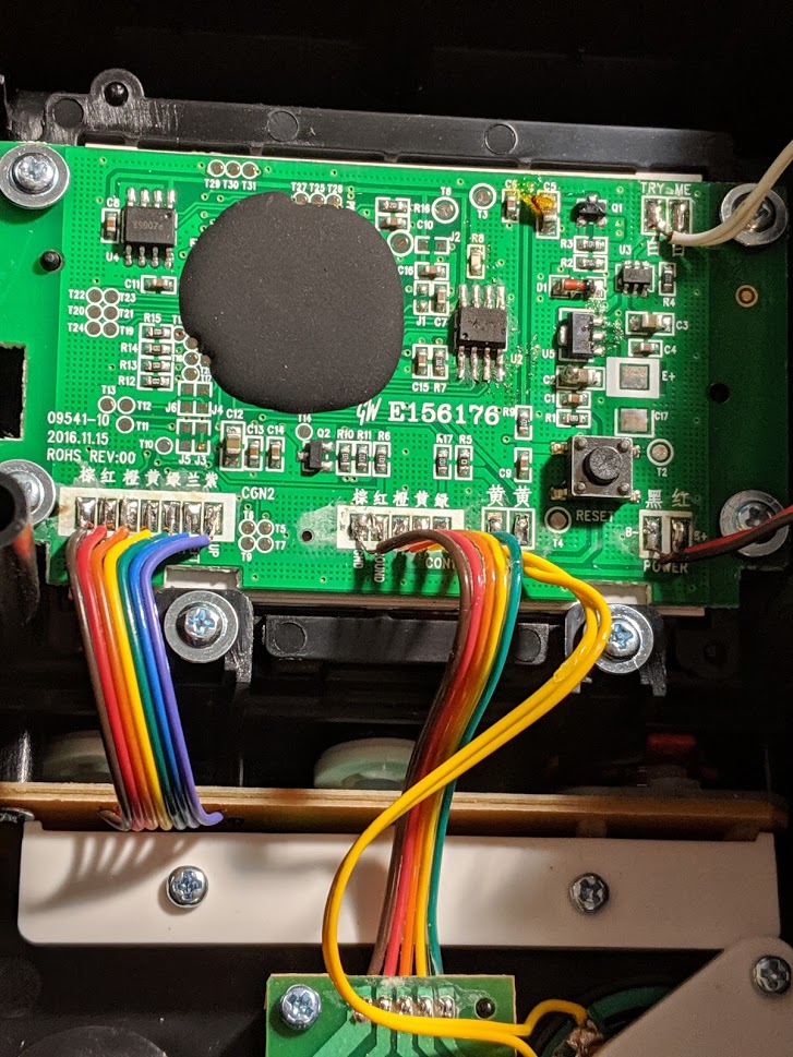
According to some other folks who had previously taken a look at these, the component covered in epoxy is essentially a NES on a chip (NOAC). Aside from that we have see two TSOP 8 packages on the board and that’s about it!
What to do from here
The goal of this and upcoming posts is see if we can get a dump of any external storage, and possible flash other ROMS to this cabinet, if it’s a NOAC we may be able to flash other NES roms onto it. Perhaps we can hack together a software mod that will allow us to swap between ROMs on the same cabinet (assuming that the proper controls are present)
Now What?
When looking at any embedded system from a reverse engineering perspective, one of the first things you do is try to catalog all of the components present. Luckily for us, this target has very few onboard components and one of them even has a part number that we can google!
Looking at the chip slightly to the right of the right of the NOAC, we spot the part number Winbond 25Q16VNIQ. This part number is very familiar to me, so no googling was required, this is a SPI EEPROM!
- Q: Why do we care?
A: This chip is likely used for non-volatile storage, we may be able to extract the information from this chip to begin analyzing the ROM!
- Q: What the heck is SPI?
- A: SPI stands for Serial Peripheral Interface this is a common protocol used in embedded systems.
For those that are not familiar with SPI, I will give a brief overview of how it works, there are plenty of great resources and videos online that will provide a much better explanation.
- It should be noted that in later iterations of these cabinets, the part numbers are slightly different!
SPI
The SPI bus requires 4 pins (there is a QUAD SPI mode that can also be used but we’ll cover the basics first)
| Pin | Usage |
|---|---|
| CS (Chip Select) | Used to select the appropriate device on the SPI bus that the host wishes to communicate with |
| CLK (Clock) | Clock signal that is host generated, data is sampled on the Rising edge of the clock |
| MOSI (Master out slave in) | This line is used to send data to the target device from the host devices, we will issue commands through this line |
| MISO (Master in slave out) | Responses from the target device will be sent over this line |
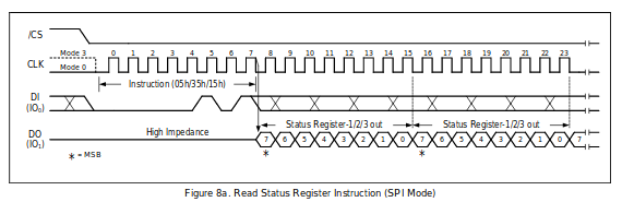
In order to access a SPI device, the following sequence occurs:
- The host (in out case the NOAC), will pull the CS line low, this alerts the target that the host wishes to communicate
- The host will then provide a clock signal to the target device
- The host provides an instruction over the MOSI line (this varies based on the operation you wish to perform)
- The host continues to provide a clock signal while waiting for a response on the MISO line.
The picture below (taken from the WINBOND datasheet) outlines this sequence nicely
Using the SPI protocol we can read out the pages of this EEPROM. There are multiple ways that this can be done and we’ll talk about a few in later posts:
- Read out SPI flash using an Arduino and writing our own firmware
- Use the linux_spi driver with a beaglebone black or Raspberry Pi
- Buspirate with the flashrom software
Attempted Extraction 1 via Arduino
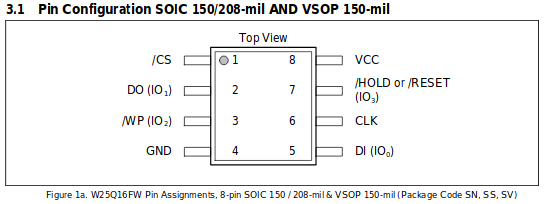
I desoldered the SPI flash with a hot air station and placed it in a breakout socket - using the following diagram for reference I connected it to the Arduino’s SPI controller:

I used an Arduino to issue the SPI commands to read pages from the EEPROM. While this worked, it took a long time to read out as I had to read the pages from the SPI chip and send those over a serial link back to a program on my computer. This was a useful exercise for multiple reasons, writing a program to issue the commands directly gave me more insight as to how SPI worked and I gained familiarity with an Arduino library. It’s never a bad idea to get a little more hands on experience with an embedded protocol.
Using the EEPROM utility I wrote for the Arduino allowed me to read / write from the EEPROM using a simple python program on my host machine. The only problem with this is that it took some time, and readouts were inconsistent (almost certainly faults on my end). Some example code for reading the chip ID can be seen below, just to give an understanding of how to utilize the Arduino SPI libraries
1
2
3
4
5
6
7
8
9
10
11
12
13
14
15
16
17
18
19
20
21
22
23
24
25
26
27
28
29
30
31
32
33
34
#include <SPI.h>
const byte INSTREAD  = B0000011;
const byte INSTWRITE = B0000010;
const byte INSTWREN  = B0000110;
const byte INSTWRDI  = B0000100;
const byte READID = B10011111;

const int chipSelectPin = 10;
void setup()
{
  Serial.begin(9600);
  // start the SPI library:
  SPI.begin();
  SPI.setBitOrder( MSBFIRST );
  pinMode(chipSelectPin, OUTPUT);
}

unsigned int get_chip_id()
{
  unsigned int id = 0;
  // First, select our ship
  digitalWrite(chipSelectPin, LOW);
  // Issue the READID command (Pulled from datasheet (standard))
  SPI.transfer(READID);
  // Clock the response back from the chip, each transfer is 8 bytes!
  id = SPI.transfer(0);
  id = (id << 8) || SPI.transfer(0);
  id = (id << 8) || SPI.transfer(0);
  Serial.println(id,HEX);
  // Release CS pin as we are done with this transaction
  digitalWrite(chipSelectPin, HIGH);
  return id;
}
However,I found the Flashrom utility in another blog post and decided to move forward with that instead. This was the one that worked best for me, and was the most consistent so we will cover that in this post. If there is interest I will write another post abut the first two methods and my attempts at using them! (I think it’s important to highlight the things you try that don’t work, we’re not all rockstars after all!)
Buspirate / Flashrom
The buspirate can be thought of as a multitool for hardware hacking and reversing. It comes out of the box with lots of features and supported protocols that make hardware analysis much easier and more streamlined.
Flashrom is a tool that has been developed to assist in dumping and extracting various storage mediums (such as our target EEPROM) and has support for a large amount of programmer hardware. We will be using the buspirate as the “programmer” for our example. It’s a great project that I’ve used countless times for tasks just like this.
Building Flashrom (On Ubuntu 19.04)
If you wish to build flashrom from source, the steps can be seen below:
- Clone the source:
git clone https://github.com/flashrom/flashrom.git
- Enter the directory:
cd flashrom
- Install dependencies:
sudo apt-get install build-essential libpci-dev libusb-dev libusb-1.0-0-dev
- Make / Make Install:
sudo makethensudo make install
Dumping the flash
If we can manage to extract the data from this chip then we will have a great starting point, however there are sometimes issues with extracting SPI flash chips:
- Some have built in security mechanisms that can disable readouts
- Reading and writing in circuit can prove to be troublesome due to signal integrity issues that arise.
- When powering the chip, we may inadvertantly power other things on the board that will try to access it
- The traces on the board may cause reflection issues and result in inconsistent reads / writes
Before we worry about any of those issues, we need to connect the Buspirate to the chip, we’ll use one of these clips
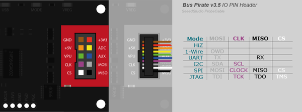
Remember since this is a SPI flash, we need four pins: CS,CLK,MISO,MOSI. We will also need to provide a common ground for the reader and our cabinet. Using the pinout seen below (pulled from the datasheet) we can connect the appropriate pins from our clip to the buspirate. The breakout pins on the bus pirate are conveniently labeled for us so it’s just a matter of matching them up!
Once the clip is attached to the chip as seen below, we can try to run flashrom and get a dump of the EEPROM!

Flashrom is run as follows:
1
2
3
4
5
6
7
8
wrongbaud@wubuntu:~/blog/cab-work$ sudo flashrom -p buspirate_spi:dev=/dev/ttyUSB0 -r rampage-cabinet.bin
flashrom v1.1-rc1-2-g93db6e1 on Linux 5.0.0-15-generic (x86_64)
flashrom is free software, get the source code at https://flashrom.org
Using clock_gettime for delay loops (clk_id: 1, resolution: 1ns).
Bus Pirate firmware 6.1 and older does not support SPI speeds above 2 MHz. Limiting speed to 2 MHz.
It is recommended to upgrade to firmware 6.2 or newer.
Found GigaDevice flash chip "GD25Q80(B)" (1024 kB, SPI) on buspirate_spi.
Reading flash... done.
Success! It seems to have worked!
The arguments are pretty straightforward:
-pis used for the programmer, in our case this is the buspirate located at/dev/ttyUSB0-ris used to indicate that we wish to read out this EEPROM intorampage-cabinet.bin
Taking a look at the results
To close out, let’s open up the resulting blob in a hex editor and compare the contents to the Rampage NES rom…
When we search for the first 0x100 bytes of the Rampage NES rom, we find them in two locations in the binary dump as shown below:
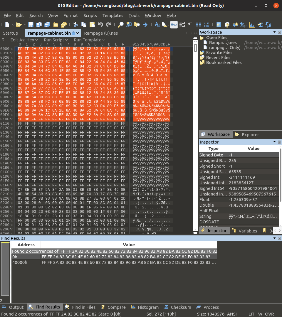
The start of the rom is located at offset 0 and offset 0x40000, this type of repeated patter is fairly common in embedded systems and sometimes used as a backup method.
Blog Updates (as of 2022):
Future blog posts and entries can be found here.
If you are interested in learning more about reverse engineering check out my 5 day hardware hacking course, public and private offerings are available upon request
Never want to miss an update or blog post? Check out my mailing list for a quarterly newsletter about reverse engineering embedded devices