

BasicFUN MK Teardown Part 1: Flash Extraction
Background
I noticed not too long ago that a new BasicFUN cabinet came out featuring one of my favorite childhood games: Mortal Kombat. This of coursed piqued my interest and I decided to purchase one and perform a teardown and hopefully dump the flash!
One thing that is important to note is that unlike the previous cabinets and roms that we looked at that were based on consoles that contained 6502 CPUs, the current opinion of people on the forums are saying that this is the Sega Genesis port of Mortal Kombat, meaning that if we manage to extract the storage of this platform we can disassemble some 68k code! The Sega Genesis was my only console growing up and I’ve reversed many Megadrive/32x ROMs - so needless to say I was excited to extract some data from this platform.
Blog Updates (as of 2022):
- Future blog posts and entries can be found here.
- If you are interested in learning more about reverse engineering check out my 5 day hardware hacking course, public and private offerings are available upon request
- Never want to miss an update or blog post? Check out my mailing list for a quarterly newsletter about reverse engineering embedded devices
Initial Teardown
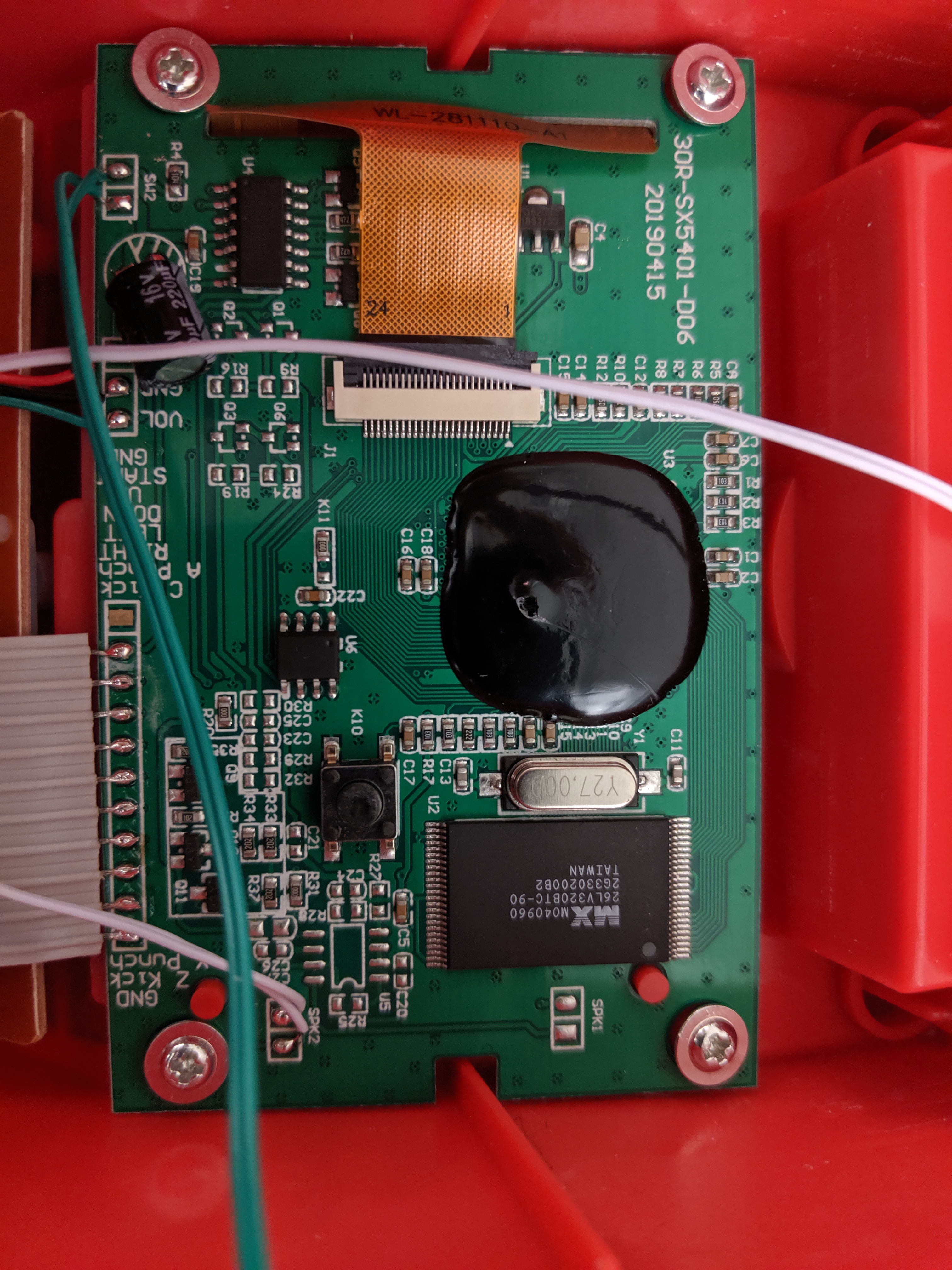
Taking a look at the PCB, you’ll notice that something is very different than the other boards. Instead of an 8 pin SPI flash, we have a much larger chip with many more pins. This is a parallel flash chip, and it operates in a different manner than the SPI flash chips that we’ve extracted previously, lets start by explaining how parallel flash chips work.
Understanding Parallel Flash
Parallel flash chips are very different than the storage mediums we’ve looked at in the past. They have dedicated address and data lines that are used to access data at certain specific addresses on the chip, rather than accessing the data sequentially like other flash ROMs we’ve talked about in the past. See the pinout below from the relevant datasheet for this chip:
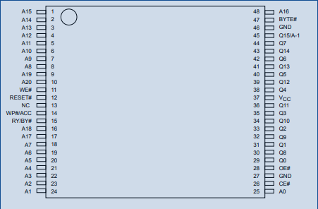
Let’s start by pointing out the pins that are most important for doing a readout according to the datasheet
I would highly recommend you read along with the datasheet open, having the ability to properly read and interpret a datasheet is very useful when reversing hardware or doing embedded design! I will only be covering a few aspects about how these chips work with this post and there are a lot more features that you may need at some point!
| Pin Name | Purpose |
|---|---|
| OE:Output Enable | This pin is asserted when we want data to be output from the chip |
| CE: Chip Enable | This pin is used to control the internal state machine of the flash |
| WE: Write Enable | This pin is used when a write operation is performed |
| BYTE: Byte mode | This pin is used in to enable the reading of individual bytes, otherwise two bytes are read and written at a time |
| A0:A21 / Address Pins | These pins are all used to determine what address to read or write to based on the state of the flash chip |
| D0:D16 / Data Pins | These are used to input or output data based on the state of the chip |
In order to perform a read operation, the following things should be done in order
- Pull CE (chip enable) to GND
- Write the address to be read on the address lines A0:AX
- Pull OE (output enable) to GND
- Read the bytes (or byte depending on the state of the BYTE pin) on the D0:D16 lines
Note that all of these things have to be done within an appropriate time window that is outlined in the diagram below from the datasheet:
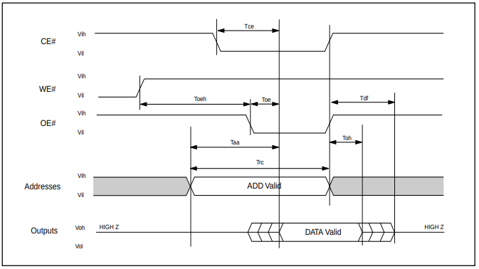
Alright so we have a rough outline of how to perform read operations on the chip, nothing horribly complicated, aside from the amount of pins needed!
Dumping the Parallel flash with an ESP32
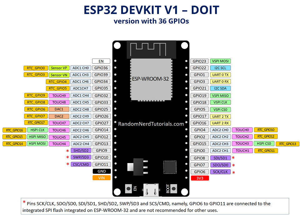
For this post, we’re going to dump this flash using the ESP32 microcontroller. This is a very popular and well supported MCU that houses plenty of embedded peripherals as well as a wireless SoC that can be used for Bluetooth and WiFi communications. Below is a link to the development board we’ll be using as well as a pinout.
So next you’re probably wondering, “How on earth are we going to extract information from this chip when we need so many data and address lines!?” Well, luckily for us there are a number of ways that we can use external ICs (integrated circuits) to expand the amount of IO pins that we can use!
In order to expand our IO capabilities to be able to interact with this flash chip we are going to use an I2C based IO expander chip called the MCP23017. This chip, as the name suggests, can be communicated with I2C and can be configured to read or write to 16 individual GPIO pins. We can also put multiple MCP23017 chips on the same I2C bus meaning that we will be able to interact with 48 pins just using I2C on the ESP32! The datasheet for the MCP23017 can be found below.
Before we get involved with how this particular chip works, we will provide a brief overview of I2C for the unfamiliar.
Understanding I2C
In previous posts, we discussed UART and SPI, these two protocols are somewhat limited when it comes to addressing multiple devices at once. For example, UART has no selection or addressing capability, and SPI requires the CS line to be pulled low which will quickly start to eat up GPIO lines with using multiple SPI chips on the same bus.
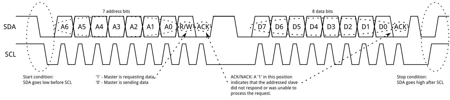
I2C uses two lines for communication Serial Data (SDA) and Clock (SCL). I2C is similar to SPI in that is synchronous, with the sampling being based on the SCL signal. One benefit of I2C is the ability to address certain chips on the bus within the I2C message frame. A brief overview of the message structure can be seen below:
| Start Condition | Address Frame | R/W Bit | ACK/NACK | Data Frame | ACK/NACK | Data Frame 2 | ACK/NACK | Stop Bit |
|---|---|---|---|---|---|---|---|---|
| 1 Bit (H->L Transition) | 7 or 10 bits | 1 bit | 1 bit | 8 bits | 1 bit | 8 bites | 1 bit | 1 bit |
The address for an I2C slave is typically controlled by asserting IO lines on the chip. For example on the MCP23017 chip pins 15:17 control the lower bits of the address variable. We will use these to allow us to have 3 MCP23017 chips on the I2C bus connected to the ESP32, using addresses 0x20,0x21 and 0x22
The R/W bit (read / write) is used to determine the type of operation that will be performed on the I2C device. For example you may write to a register of an I2C based sensor in order to configure or initialize it, after that you would read the data from it. We’ll need to read and write from the MCP23017 chips in order to properly dump the parallel flash chip.
See the example be low from the Sparkfun I2C tutorial for a better explanation!
Interfacing with the MCP23017
In order to properly talk to this parallel flash chip, we will use two MCP23017 chips to control the address lines and one to read from the data lines. Next we’ll look at how to configure the MCP23017 chips via their internal registers. All of the data from below has been pulled from the datasheet below:
The MCP23017 has a series of internal registers that are used to configure the state and direction of the 16 GPIO lines. The datasheet outlines all of this information nicely but for our purposes we only need to interract with the following:
| Addr | Reg | Purpose |
|---|---|---|
| 0x00 | IODIRA | Set the direction of the pin bank (input or output) |
| 0x01 | IODIRB | Set the direction of the pin bank (input or output) |
| 0x12 | GPIOA | Set or get the value of the pins based on direction |
| 0x13 | GPIOB | Set or get the value of the pins based on direction |
In order to set these registers, we need to perform the following with the ESP32:
- Send an I2C write packet, with the address of the target chip that we want to talk to.
- Wait for the ACK from the target chip
- Write the address of the register that we want to access
- Write the value that is desired at the previously written address
The image below, perfectly outlines what we are doing when we interract with something over I2C:

And this is how we will perform that using the ESP32!
1
2
3
4
5
6
7
8
9
10
11
12
13
14
15
16
//Write a value to a command register
esp_err_t write_mcp_register(int mcp_addr,int reg_addr, int reg_value){
    esp_err_t i2c_ret = ESP_OK;
    i2c_cmd_handle_t cmd = i2c_cmd_link_create();
    i2c_master_start(cmd);
    // Select the chip we want to talk to via the I2C address set with the ADDR pins
    i2c_master_write_byte(cmd,mcp_addr<<1|WRITE_BIT,1);
    // Write the address of the register that we want to manipulate
    i2c_master_write_byte(cmd,reg_addr,1);
    // Finally write the value that we want at that register
    i2c_master_write_byte(cmd,reg_value,1);
    i2c_master_stop(cmd);
    i2c_ret = i2c_master_cmd_begin(I2C_NUM_0,cmd,(1000/portTICK_RATE_MS));
    i2c_cmd_link_delete(cmd);
    return i2c_ret;
}
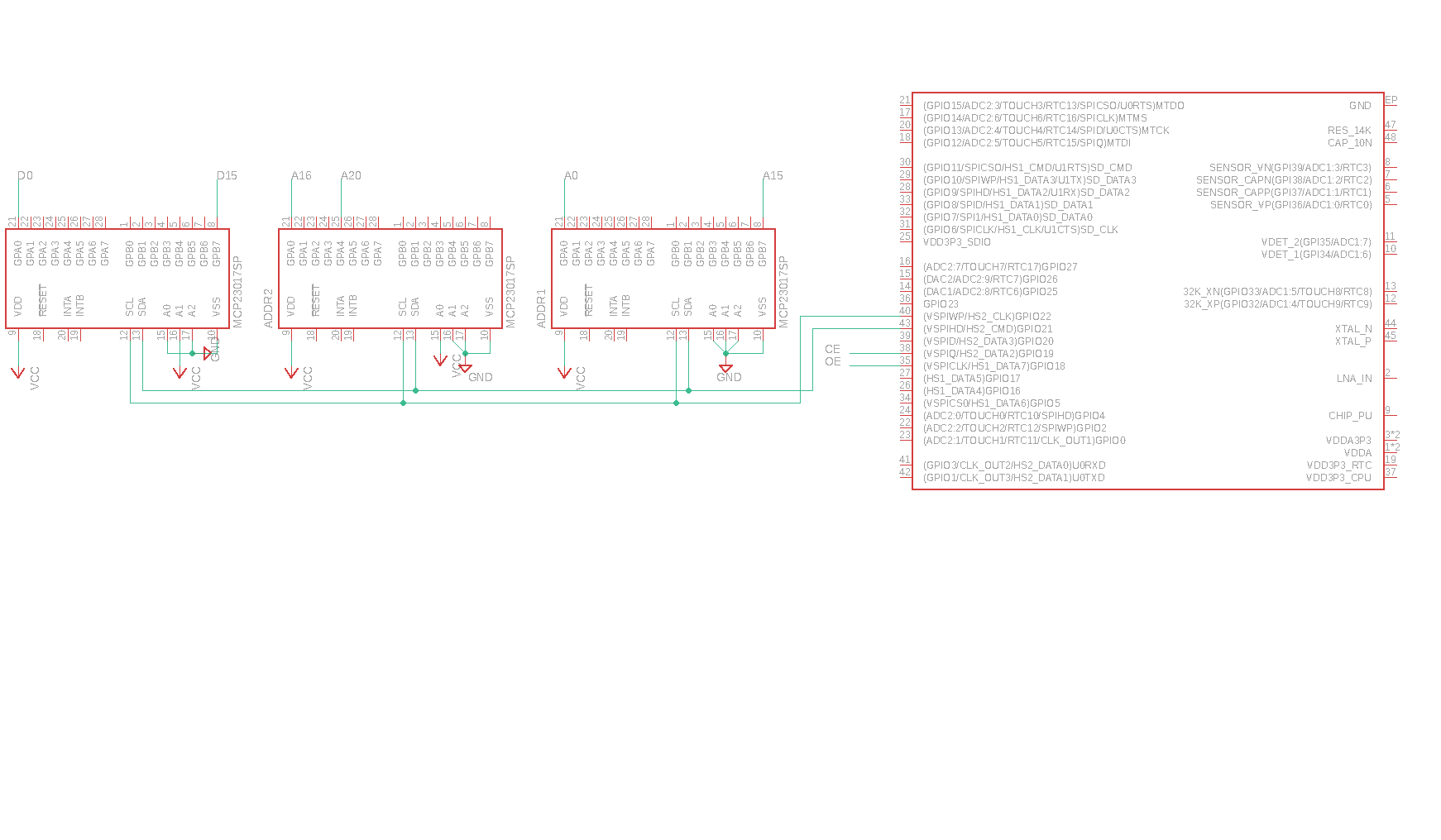
So what we will have to do with these IO expanders is use 2 for the address lines,since we need 20 address lines total and a third for the 16 data lines. We can wire all of these up to the ESP32 as shown in the eagle diagram below:
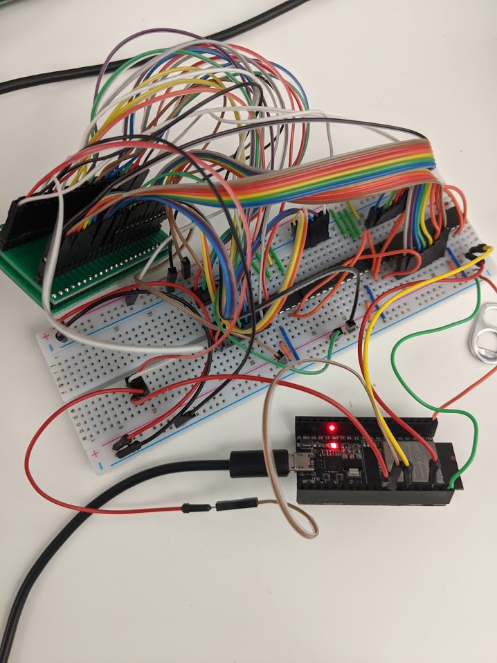
And this is what it looks like on the bench, using a TSOP48 breakout board
Also below is a table outlining the addresses for each chip and what it’s used for:
| I2C Addr | Purpose/Target Flash Pins |
|---|---|
| 0x20 | A0:A15 |
| 0x21 | A16:A20 |
| 0x22 | D0:D15 |
These addresses are set using the ADDR pins on the MCP20317, the three lines correspond to the lower bits of the address, you can see how these are set in the above diagram.
With this snippet of code, we configure the three MCP chips using our write_mcp_register function:
1
2
3
4
5
6
7
8
9
10
11
12
13
14
15
16
17
18
void mcp_configure(){
    // Set the bits of the first MCP chip to output mode (addr 0:15)
    write_mcp_register(MCP_ADDR_1,GPIOA,0);
    write_mcp_register(MCP_ADDR_1,GPIOB,0);
    write_mcp_register(MCP_ADDR_1,IODIRA,0);
    write_mcp_register(MCP_ADDR_1,IODIRB,0);

    // Set the bits of the second MCP chip to output mode (addr 16:20)
    write_mcp_register(MCP_ADDR_2,GPIOA,0);
    write_mcp_register(MCP_ADDR_2,GPIOB,0);
    write_mcp_register(MCP_ADDR_2,IODIRA,0);
    write_mcp_register(MCP_ADDR_2,IODIRB,0);


    // Configure the pins to be connected to the data lines to be input pins
    write_mcp_register(MCP_DATA,IODIRA,0xFF);;
    write_mcp_register(MCP_DATA,IODIRB,0xFF);
}
With the first two chips properly configured for output, if we want to write a full 20 bit address value out using the ESP32, the followng code will suffice
1
2
3
4
5
6
7
8
void MXICWriteAddr(int address){
    // Write the low 8 bits out to GPIOA of the first MCP23017 chip at 0x20
    write_mcp_register(MCP_ADDR_1,GPIOA,(address&0xFF));
    // Write the next 8 bits out to GPIOB of the first MCP23017 chip at 0x20
    write_mcp_register(MCP_ADDR_1,GPIOB,((address>>8)&0xFF));
    // Write the last 4 bits out to GPIOA of the second MCP23017 chip at 0x21
    write_mcp_register(MCP_ADDR_2,GPIOA,((address>>16)&0xFF));
}
And we can perform a read of D0:D16 using our third MCP23017 chip (which has been set to input mode) with the following code:
1
2
3
4
5
6
7
8
9
10
11
12
13
14
15
16
17
18
19
20
21
22
23
24
25
26
27
void MXICReadData(int mcp_addr,int flash_addr){
    uint8_t dath = 0;
    uint8_t datl = 0;
    esp_err_t i2c_ret = ESP_OK;
    // Perform a write operation to tell the IC what register we want to read from
    i2c_cmd_handle_t cmd = i2c_cmd_link_create();
    i2c_master_start(cmd);
    i2c_master_write_byte(cmd,mcp_addr<<1|WRITE_BIT,1);
    i2c_master_write_byte(cmd,GPIOA,1);
    i2c_master_stop(cmd);
    i2c_ret = i2c_master_cmd_begin(I2C_NUM_0,cmd,(.1/portTICK_RATE_MS));
    i2c_cmd_link_delete(cmd);
    // Now read from the IC at the given register, subsequent reads will increment the address value automatically
    cmd = i2c_cmd_link_create();
    i2c_master_start(cmd);
    i2c_master_write_byte(cmd,mcp_addr<<1|READ_BIT,1);
    i2c_master_read_byte(cmd,&dath,0);
    i2c_master_read_byte(cmd,&datl,1);
    i2c_master_stop(cmd);
    i2c_ret = i2c_master_cmd_begin(I2C_NUM_0,cmd,(.1/portTICK_RATE_MS));
    i2c_cmd_link_delete(cmd);
    //Print the data out over serial
    printf("%X:%X:",dath,datl);
    if(flash_addr % 16 == 0){
        printf("\r\n");
    }
}
Dumping the Flash using the MCP23017
Alright, so now that we have our MCP23017 chips wired up to the flash chip as shown in the diagram, what’s next? All we need to do is follow the timing diagram above and perform the following:
- Pull CE Low
- Write our address value out over I2C, using our two MCP23017 chips at I2C addresses 0x20,0x21
- Pull OE Low
- Read the result in using I2C using the third MCP23017 chip at I2C address 0x22
The following ESP32 function will do just this for us:
1
2
3
4
5
6
7
8
void ReadFlash(int addr){
    gpio_set_level(GPIO_CE,0);
    MXICWriteAddr(addr);
    gpio_set_level(GPIO_OE,0);
    MXICReadData(MCP_DATA,addr);
    gpio_set_level(GPIO_CE,1);
    gpio_set_level(GPIO_OE,1);
}
Now lets loop over the address space of the chip, the MXICReadData will print it out over the serial port on the ESP32 and we can reconstruct the flash using python once we have dumped it all.
1
2
3
    for(addr=0;addr<0x200000;addr++){
        ReadFlash(addr);
    }
This will dump the bytes that are read out over the serial port. While this is obviously not the most elegant solution, it will suffice for our purposes. We can reconstruct the image using the serial output with a python script.
In order to read the flash we can connect to the serial device presented by the ESP32 board we are using and log it to a file: sudo screen -L -Logfile mk-read.log /dev/ttyUSB0 115200
The following python snippet can reconstruct the binary file from the serial log
1
2
3
4
5
6
7
8
import struct
outfile = open('mk.bin','rb')
with open('mk-read.log','r') as file:
    lines = file.readlines()
    vals = lines[0].strip(":")
    for val in vals:
        outfile.write(struct.pack('B',int(val,16)))
outfile.close()
Now we can start taking apart the resulting binary file to finally see what’s on the flash, but we will save that for another post!
The full ESP32 project can be found here
Please note that there are a lot of improvements to be done and hopefully I will have the time to make these changes over the holidays.
Just as a teaser, let’s take a look at the ROM in 010Editor and see if we can find any Genesis ROM headers…
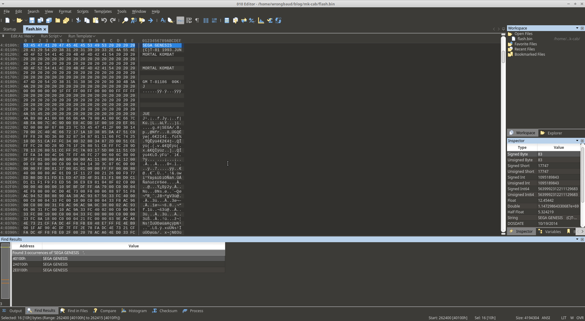
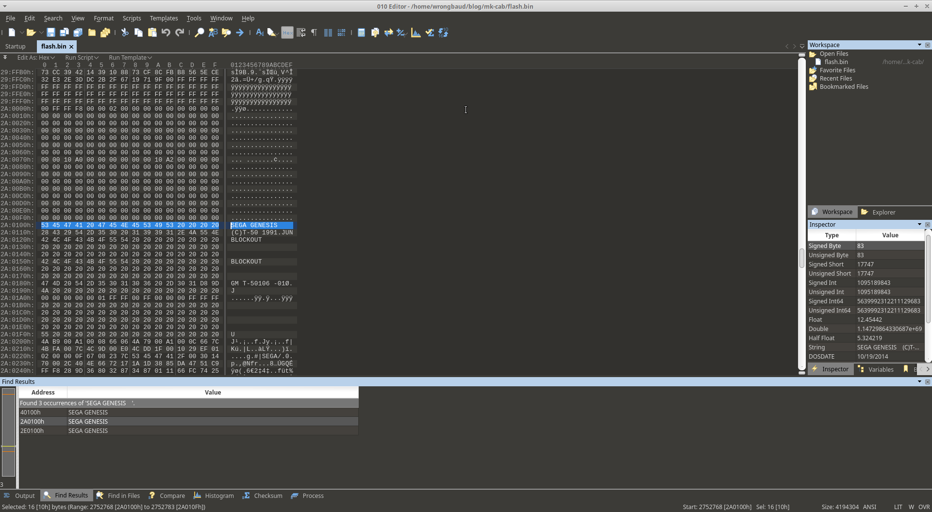

Looks like there are quite a few ROMs in here! In the next post we’ll tear these out, see if they run in emulators, and try to see what is different between the original MK rom and the one we pulled from this cabinet!
Conclusion
Thanks for bearing through this entire writeup, there was a fair amount to cover here and I wanted to make sure that it was all somewhat easy to follow. With this writeup, we’ve learned about multiplexers, I2C and how parallel flash chips work. I hope that this was useful for those that were interested and as always please reach out with any corrections or questions! Next post we will dissect the resulting binary and see what we can find!