

Background
I was looking around my apartment for potential targets for my next post and was pleasantly surprised to find the following XBox One controller still in the packaging:

I don’t really play my XBox that much so I thought it might be interesting to tear down this controller and see what kind of information we could extract from it.
Goals
When assessing an embedded platform there are a number of things you can do or try to accomplish, with this post I want to demonstrate/test the following:
- Can the firmware be extracted from the target?
- Can the target be debugged or instrumented in such a way that allows us to learn more about it’s internal operations?
- Can the firmware be modified or changed, either through software exploitation or hardware modifications?
The first step to answering some of these questions will be a hardware teardown.
Hardware Teardown
Opening up the case reveals the following PCB:
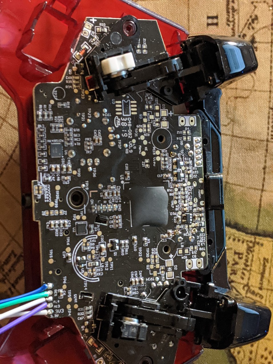
Note that there really isn’t too much to see here, as the main chip is covered in epoxy. Luckily for us a lot of the test pads are labeled, but the labeled ones seem to be test points for various button presses, so there’s nothing exciting there.
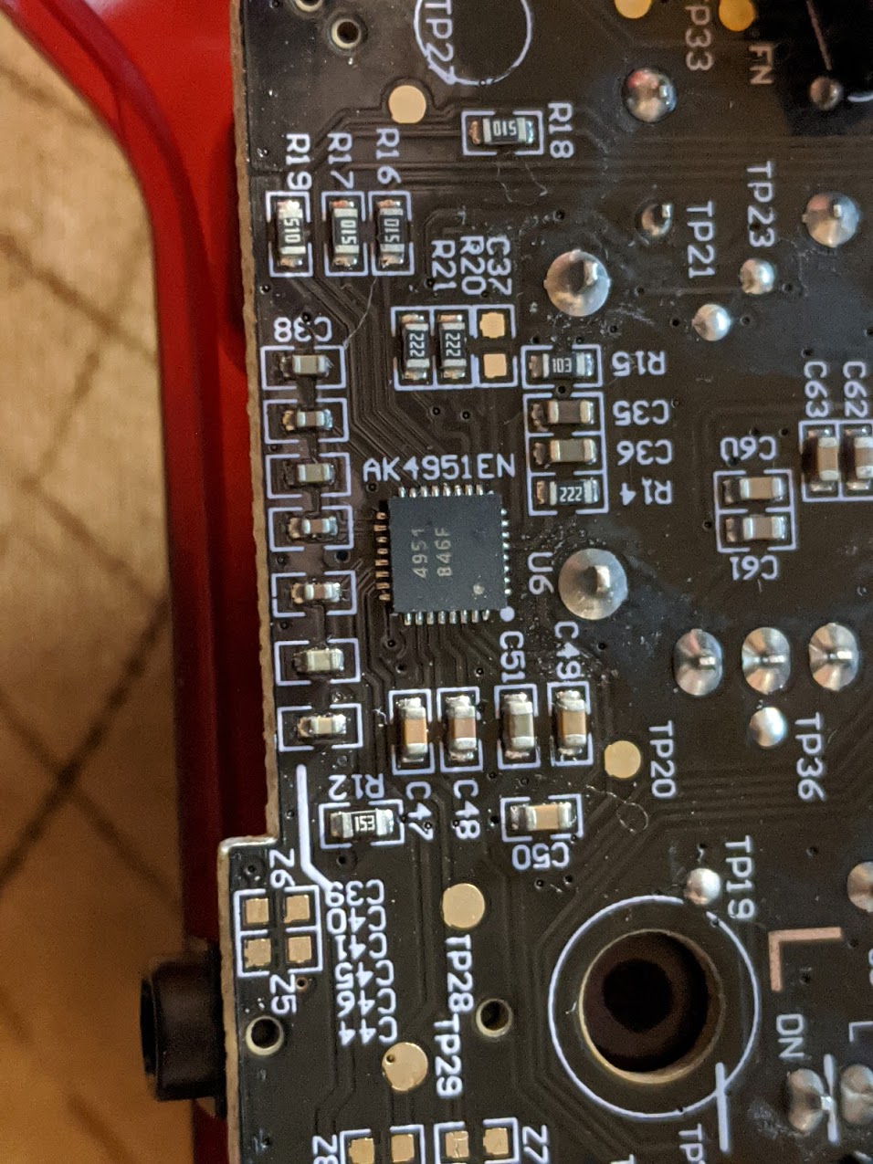
There is an IC labeled AK4961 towards the bottom of the board, but this is an audio codec chip. The datasheet can be found here. This chip is a low power 24-bit stereo CODEC with a microphone, headphone and speaker amplifiers.
If we look to the right of this however there is a small grouping of pads with some silk screen labelling:
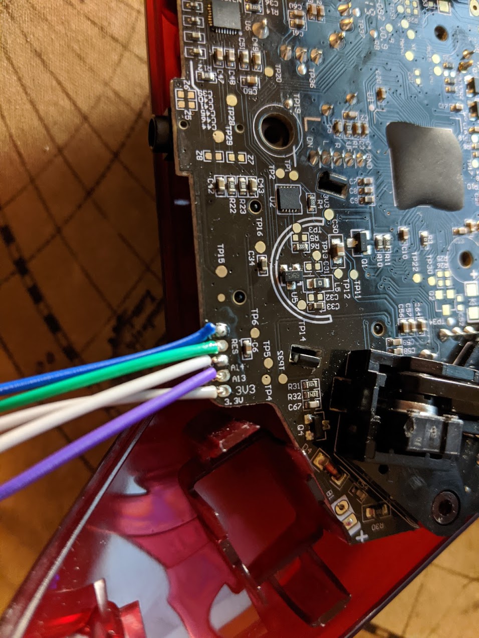
So we see 3V3,A13,A14,RES labeled in the silkscreen. This is worth taking a look at, and if you’ve read my previous post about the router teardown and discovering UARTs you may already have some ideas on how to proceed here. We’ll start by measuring the voltage of each pin with a multimeter:
| Pin | Value |
|---|---|
| 0/NA | 0 (GND) |
| RES | 3.3V |
| A14 | 0.1V |
| A13 | 3.3V |
| 3V3 | 3.3V |
There was no fluctuation or modulation on RES, A14 or A13, so these must be for something else, but what? Given that one of the labels is RES (which likely stands for system reset) there is a good chance that there are JTAG or SWD headers.
We can test if the RES pin actually resets the target by pulling it low with a 10k resistor (remember we’re reversing things here and don’t want to accidentally short something!). If you are not familiar with these types of headers or how a system reset pin typically works - they are often active low meaning that they idle at a high value and have to be pulled low to be activated. So if we monitor the output of dmesg -w and toggle this line low with a 10k resistor, what do we see?
1
2
3
4
5
6
7
8
9
10
11
12
13
14
15
[ 2108.588884] usb 1-6.4: new full-speed USB device number 10 using xhci_hcd
[ 2108.691108] usb 1-6.4: New USB device found, idVendor=0e6f, idProduct=02a2, bcdDevice= 1.0f
[ 2108.691113] usb 1-6.4: New USB device strings: Mfr=1, Product=2, SerialNumber=3
[ 2108.691116] usb 1-6.4: Product: PDP Wired Controller for Xbox One - Crimson Red
[ 2108.691119] usb 1-6.4: Manufacturer: Performance Designed Products
[ 2108.691122] usb 1-6.4: SerialNumber: 0000AE38D7650465
[ 2108.698675] input: Generic X-Box pad as /devices/pci0000:00/0000:00:14.0/usb1/1-6/1-6.4/1-6.4:1.0/input/input25
[ 2131.403862] usb 1-6.4: USB disconnect, device number 10
[ 2133.420350] usb 1-6.4: new full-speed USB device number 11 using xhci_hcd
[ 2133.522469] usb 1-6.4: New USB device found, idVendor=0e6f, idProduct=02a2, bcdDevice= 1.0f
[ 2133.522474] usb 1-6.4: New USB device strings: Mfr=1, Product=2, SerialNumber=3
[ 2133.522478] usb 1-6.4: Product: PDP Wired Controller for Xbox One - Crimson Red
[ 2133.522480] usb 1-6.4: Manufacturer: Performance Designed Products
[ 2133.522483] usb 1-6.4: SerialNumber: 0000AE38D7650465
[ 2133.530103] input: Generic X-Box pad as /devices/pci0000:00/0000:00:14.0/usb1/1-6/1-6.4/1-6.4:1.0/input/input26
Ah excellent, doing this caused the controller to reset, that’s one pin down, 2 more to go.
When looking at debug headers like this, a common assumption is that it’s for JTAG or some other form of hardware level debugging. However, the JTAG spec requires that there be at least 4 pins, TDO,TDI,TMS and TCK. We only have two on our target, so there is a good chance that this is a Single Wire Debug (SWD) port.
Understanding SWD
SWD is a common debugging interface that is used for ARM Cortex targets. As the name implies, SWD only requires one data line and one clock line, but how can we determine which one is which? Before we go down that route, we should understand a little more about how SWD works and what tools can be used to interface with it.
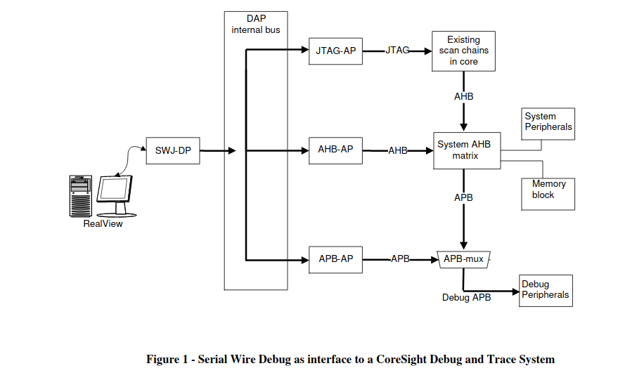
First off - SWD interfaces with something called a “Debug Access Port” (DAP). The DAP brokers access to various “Access Ports” (APs) which provide functionality including from typical hardware debugging, legacy JTAG cores, and other high performance memory busses. The image below pulled from this document provides a visual representation of how the DAP and APs are architected.
Each of these APs consist of 64, 32 bit registers, with one register that is used to identify the type of AP. The function and features of the AP determine how these registers are accessed and utilized. You can find all of the information regarding these transactions for some of the standard APs here. The ARM interface specification defines two APs by default and they are the JTAG-AP, and the MEM-AP. The MEM-AP also includes a discovery mechanism for components that are attached to it.
SWD Protocol
As we mentioned before - SWD was developed as a pseudo-replacement for JTAG. With SWD the pin count was reduced from 4 to 2 and it provides a lot of the same functionality of JTAG. One downside to SWD however is that devices can not be daisy chained together, which JTAG allowed for. The two pins that are used in SWD are below:
| Pin | Purpose |
|---|---|
SWCLK | Clock signal to CPU, determining when data is sampled and sent on SWDIO |
SWDIO | Bi directional data pin used to transfer data to and from the target CPU |
SWD utilizes a packet based protocol to read and write to registers in the DAP/AP and they consist of the following phases:
- Host to target packet request
- Bus turnaround
- Target to host acknowledgment response
- Data transfer phase
The packet structure can be seen in the image below, I’ve broken out the various fields in the table as well.
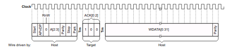
| Field | Usage |
|---|---|
| Start | Start bit, value 1 |
| APnDP | This bit indicates whether the Debug Port access register or the Access Port access register is to be used. |
| RnW | Read / Write bit |
| A[2:3] | Address field for the AP or DP address |
| Parity | Parity bit for all packet requests |
| Stop | Stop bit (always 0) |
| Park | Line to be driven high during the turnaround period |
| ACK[0:2] | Ack bits from the target back to the host |
| DATA[0:32] | The actual data frame, which will be either read from the target or written to the target depending on the RnW bit |
| Parity | Final parity bit for the data frame |
After the park bit (from the host to the target) there is a turnaround period, which basically means that the target will now respond on the same line.
From an extremely high level, the SWD port uses these packets to interface with the DAP, which in turn allows access to the MEM-AP which provides access to debugging as well as memory read / write capabilities. For the purposes of this post we will use a tool called OpenOCD to perform these transactions. We will review how to build and use OpenOCD next.
OpenOCD
Install the dependencies:
1
sudo apt-get install build-essential libusb-1.0-0-dev automake libtool gdb-multiarch
Clone the repository, configure, and build!
1
2
3
4
5
wrongbaud@115201:~/blog$ git clone https://git.code.sf.net/p/openocd/code openocd-code
cd openocd-code
./bootstrap
./configure
make -j$(nproc)
With OpenOCD built, we can attempt to debug this controller over SWD. In order to do this we need to tell OpenOCD at least two things:
- What are we using to debug with (which debug adapter are we using)
- What target are we debugging
To do the debugging, we will use the FT2232H which we used in a previous post to dump a SPI flash. With this interface we can use OpenOCD to query information about the target via SWD, which is important because at this stage in the reversing process we don’t even know what the target CPU is!
Below is a table for determining what pins on the FT2232H need to be connected to a SWD target:
| FT2232H Pin | SWD Target |
|---|---|
AD1 | SWD |
AD0 | SCLK |
AD4 | SRST (System Reset) |
Lastly, in order to use the FT2232H as a SWD adapter, you have to put a 470 OHM resistor between AD1/AD2 on the FT2232H.
Once we have the pins on the FT2232H hooked up to the target we can use the following script to query the DPIDR register on the DAP controller:
1
2
3
4
5
6
7
8
9
10
11
12
13
14
15
16
17
18
19
20
# We are using an FT2232H so specify this here
interface ftdi
# Provide the VID/PID of the FT2232H
ftdi_vid_pid 0x0403 0x6010
# There are two channels, this is the default
ftdi_channel 0
# To the best of my knowledge, this is used to properly set and confiture the state of the lines we are using
ftdi_layout_init 0x0018 0x05fb
# Enable SWD for the lines that we are using, and the port
ftdi_layout_signal SWD_EN -data 0
# This is used to specify the sRST pin, in our case we're using
ftdi_layout_signal nSRST -data 0x0010
# Here we are selecting SWD as opposed to another transport layer such as JTAG
transport select swd
# Set the speed of the adapter, this will vary based on what your hardware supports
adapter_khz 100
# Create a new dap, (TAP for JTAG terms) with name chip and role CPU, -enable let's OpenOCD to know to add it to the scan
swd newdap chip cpu -enable
# Create the DAP instance, this must be explicitly created according to the OpenOCD docs
dap create chip.dap -chain-position chip.cpu
We can run this script with openocd as shown, with the following output (note that the first time it was run, there was no output, after swapping the SWD/SCLK lines the following output was printed out). See the table below for the connections to be made to the controller from the FT2232
| FT2232H Pin | Controller |
|---|---|
AD1 | SWD (A13) |
AD0 | SCLK (A14) |
AD4 | SRST (RES) |
1
2
3
4
5
6
7
8
9
10
11
wrongbaud@wubuntu:~/blog/stm32-xbox$ sudo openocd -f openocd.cfg
Open On-Chip Debugger 0.10.0+dev-01040-ge7e681ac (2020-01-27-18:55)
Licensed under GNU GPL v2
For bug reports, read
        http://openocd.org/doc/doxygen/bugs.html
Info : FTDI SWD mode enabled
Info : Listening on port 6666 for tcl connections
Info : Listening on port 4444 for telnet connections
Info : clock speed 100 kHz
Info : SWD DPIDR 0x2ba01477
Warn : gdb services need one or more targets defined
Excellent! We’ve found a chip ID of 0x2ba01477 if we google this ID we see lots of hits for various Cortex M / STM32 devices - which would make sense because this processor series supports SWD. Now that we can communicate with the DAP, we should see if we can determine the exact processor that is being used - if this is one that has a configuration file written for it we will be able to dump flash banks and get other auxiliary information from the target processor. With this additional information we can tell OpenOCD to create a target, using the chip with the Cortex M definition, this will hopefully allow us to take more advantage of the DAP and get access to some of the more generic features while we try to figure out exactly which CPU we’re targeting:
1
2
3
4
5
6
# Set up the GDB target for the CPU, cortex_m is the CPU type,
target create chip.cpu cortex_m -dap chip.dap
# init reads out all of the necessary information from the DAP, kicks off the debugging session, etc
init
# Read out the information from the DAP, including the ROM table
dap info
When we run openocd with this config file we see the following results:
1
2
3
4
5
6
7
8
9
10
11
12
13
14
15
16
17
18
19
20
21
22
23
24
25
26
27
28
29
30
31
32
33
34
35
36
37
38
39
40
41
42
43
44
45
46
47
48
49
50
51
52
53
54
55
56
57
58
59
60
61
62
63
64
wrongbaud@wubuntu:~/blog/stm32-xbox$ sudo openocd -f openocd.cfg
Open On-Chip Debugger 0.10.0+dev-01040-ge7e681ac (2020-01-27-18:55)
Licensed under GNU GPL v2
For bug reports, read
        http://openocd.org/doc/doxygen/bugs.html
Info : FTDI SWD mode enabled
Info : clock speed 100 kHz
Info : SWD DPIDR 0x2ba01477
Info : chip.cpu: hardware has 6 breakpoints, 4 watchpoints
Info : chip.cpu: external reset detected
Info : Listening on port 3333 for gdb connections
AP ID register 0x24770011
        Type is MEM-AP AHB3
MEM-AP BASE 0xe00ff003
        Valid ROM table present
                Component base address 0xe00ff000
                Peripheral ID 0x00000a0411
                Designer is 0x0a0, STMicroelectronics
                Part is 0x411, Unrecognized
                Component class is 0x1, ROM table
                MEMTYPE system memory present on bus
        ROMTABLE[0x0] = 0xfff0f003
                Component base address 0xe000e000
                Peripheral ID 0x04000bb00c
                Designer is 0x4bb, ARM Ltd.
                Part is 0xc, Cortex-M4 SCS (System Control Space)
                Component class is 0xe, Generic IP component
        ROMTABLE[0x4] = 0xfff02003
                Component base address 0xe0001000
                Peripheral ID 0x04003bb002
                Designer is 0x4bb, ARM Ltd.
                Part is 0x2, Cortex-M3 DWT (Data Watchpoint and Trace)
                Component class is 0xe, Generic IP component
        ROMTABLE[0x8] = 0xfff03003
                Component base address 0xe0002000
                Peripheral ID 0x04002bb003
                Designer is 0x4bb, ARM Ltd.
                Part is 0x3, Cortex-M3 FPB (Flash Patch and Breakpoint)
                Component class is 0xe, Generic IP component
        ROMTABLE[0xc] = 0xfff01003
                Component base address 0xe0000000
                Peripheral ID 0x04003bb001
                Designer is 0x4bb, ARM Ltd.
                Part is 0x1, Cortex-M3 ITM (Instrumentation Trace Module)
                Component class is 0xe, Generic IP component
        ROMTABLE[0x10] = 0xfff41003
                Component base address 0xe0040000
                Peripheral ID 0x04000bb9a1
                Designer is 0x4bb, ARM Ltd.
                Part is 0x9a1, Cortex-M4 TPIU (Trace Port Interface Unit)
                Component class is 0x9, CoreSight component
                Type is 0x11, Trace Sink, Port
        ROMTABLE[0x14] = 0xfff42003
                Component base address 0xe0041000
                Peripheral ID 0x04000bb925
                Designer is 0x4bb, ARM Ltd.
                Part is 0x925, Cortex-M4 ETM (Embedded Trace)
                Component class is 0x9, CoreSight component
                Type is 0x13, Trace Source, Processor
        ROMTABLE[0x18] = 0x0
                End of ROM table

Info : Listening on port 6666 for tcl connections
Info : Listening on port 4444 for telnet connections
With these new changes, we can not only interact with the DAP and MEM-AP, but we can also debug the target via GDB. We can also determine that the target CPU is an STM32F2X series because of the 0x411 part number in the MEM-AP entry:
1
2
3
4
5
6
7
8
MEM-AP BASE 0xe00ff003
	Valid ROM table present
		Component base address 0xe00ff000
		Peripheral ID 0x00000a0411
		Designer is 0x0a0, STMicroelectronics
		Part is 0x411, Unrecognized
		Component class is 0x1, ROM table
However - just for fun, what if we didn’t have access to the DAP and wanted to figure out what our target was via memory reads and writes? To figure this out, there are some memory regions that are common in STM32 CPUs that are used to store ID and flash information. With this information we can modify the OpenOCD script to read these regions and look for relevant ID information! The table below has the necessary offsets for the ID information:
| STM Series | Offset |
|---|---|
| Generic Device ID Reg | 0xE0042000 |
| STM32F0/STM32F3 | 0x1FFFF7AC |
| STM32F1 | 0x1FFFF7E8 |
| STM32F2/STM32F4 | 0x1FFF7A10 |
| STM32F7 | 0x1FF0F420 |
| STM32L0 | 0x1FF80050 |
| STM32L0/ L1 Cat.1,Cat.2 | 0x1FF80050 |
| L1 Cat.3,Cat.4,Cat.5,Cat.6 | 0x1FF800D0 |
1
2
3
4
5
6
mdw 0x1FFFF7AC 3
mdw 0x1FFFF7E8 3
mdw 0x1FFF7A10 3
mdw 0x1FF0F420 3
mdw 0x1FF80050 3
mdw 0x1FF800D0 3
When we run the updated OpenOCd script and the above commands we see the following results:
1
2
3
4
5
6
7
8
9
10
11
12
13
14
15
16
17
18
19
20
21
22
> mdw 0x1FFFF7AC 3
0x1ffff7ac: ffffffff ffffffff ffffffff

> mdw 0x1FFFF7E8 3
0x1ffff7e8: ffffffff ffffffff ffffffff

> mdw 0x1FFF7A10 3
0x1fff7a10: 006c0028 31385114 30373639

> mdw 0x1FF0F420 3
SWD DPIDR 0x2ba01477
Failed to read memory at 0x1ff0f424

> mdw 0x1FF80050 3
SWD DPIDR 0x2ba01477
Failed to read memory at 0x1ff80054

> mdw 0x1FF800D0 3
SWD DPIDR 0x2ba01477
Failed to read memory at 0x1ff800d4

>
We can get the flash size with the following command, using the flash address from the datasheet for this chip, or the repository linked above:
1
2
> mdh 0x1FFF7A22
0x1fff7a22: 0100
Now that we know the exact target, we can remove the target swd, dap and target lines from our config file, and replace them with a call to -f /usr/local/share/openocd/scripts/target/stm32f2x.cfg from the command line. This will properly enumerate the target CPU. We also know now that this STM32F2 series chip has 0x100 1kb pages of flash memory.
1
2
3
4
5
6
7
8
9
10
11
12
13
14
15
wrongbaud@wubuntu:~/blog/stm32-xbox$ sudo openocd -f openocd.cfg -f /usr/local/share/openocd/scripts/target/stm32f2x.cfg
[sudo] password for wrongbaud:
Open On-Chip Debugger 0.10.0+dev-01040-ge7e681ac (2020-01-27-18:55)
Licensed under GNU GPL v2
For bug reports, read
	http://openocd.org/doc/doxygen/bugs.html
Info : FTDI SWD mode enabled
adapter speed: 100 kHz

Info : Listening on port 6666 for tcl connections
Info : Listening on port 4444 for telnet connections
Info : clock speed 1000 kHz
Info : SWD DPIDR 0x2ba01477
Info : stm32f2x.cpu: hardware has 6 breakpoints, 4 watchpoints
Info : Listening on port 3333 for gdb connections
Now that this is working, we can dump the internal flash with the following commands:
1
2
3
4
5
6
7
8
9
10
11
> flash list
{name stm32f2x base 0 size 0 bus_width 0 chip_width 0} {name stm32f2x base 536836096 size 0 bus_width 0 chip_width 0}

> flash read_bank 0 bank0.bin
device id = 0x00016423
flash size = 256 kbytes
wrote 262144 bytes to file bank0.bin from flash bank 0 at offset 0x00000000 in 3.690861s (69.361 KiB/s)

> flash read_bank 1 bank1.bin
flash size = 512 bytes
wrote 512 bytes to file bank1.bin from flash bank 1 at offset 0x00000000 in 0.007852s (63.678 KiB/s)
We can also debug the controller with gdb using the commands below:
1
2
3
4
5
6
7
8
9
10
11
12
13
14
15
16
17
18
19
20
21
22
23
24
25
26
27
wrongbaud@wubuntu:~/blog/stm32-xbox$ gdb-multiarch
GNU gdb (Ubuntu 8.1-0ubuntu3.2) 8.1.0.20180409-git
Copyright (C) 2018 Free Software Foundation, Inc.
License GPLv3+: GNU GPL version 3 or later <http://gnu.org/licenses/gpl.html>
This is free software: you are free to change and redistribute it.
There is NO WARRANTY, to the extent permitted by law.  Type "show copying"
and "show warranty" for details.
This GDB was configured as "x86_64-linux-gnu".
Type "show configuration" for configuration details.
For bug reporting instructions, please see:
<http://www.gnu.org/software/gdb/bugs/>.
Find the GDB manual and other documentation resources online at:
<http://www.gnu.org/software/gdb/documentation/>.
For help, type "help".
Type "apropos word" to search for commands related to "word".
(gdb) set architecture arm
The target architecture is assumed to be arm
(gdb) target remote localhost:3333
Remote debugging using localhost:3333
warning: No executable has been specified and target does not support
determining executable automatically.  Try using the "file" command.
0x0800307e in ?? ()
(gdb) x/10x 0x1FFF7A10
0x1fff7a10:	0x006c0028	0x31385114	0x30373639	0xc000fcc0
0x1fff7a20:	0x0100c000	0x67ff47d2	0x05dcf000	0x04a803b3
0x1fff7a30:	0x451744b1	0xffffffff
(gdb)
So at this point, we have the flash dumped, we can debug and single step through the firmware, but … can we reflash the MCU?
If we can locate the USB descriptor strings in the firmware image and patch them, we can use that as a visible method to determine if we can patch the firmware. Let’s load up the firmware in GHIDRA and see if we can find them, the firmware image can be loaded at address 0x8000000. We know that the firmware is loaded at 0x8000000 based on the datasheet, however if we did not have the datasheet this could be determined from OpenOCD by issuing the reset halt command and single stepping through the first instruction. Luckily, this firmware image is rather small and Ghidra makes quick work of it. The strings that were seen in the dmesg output can be seen in the screenshot below:
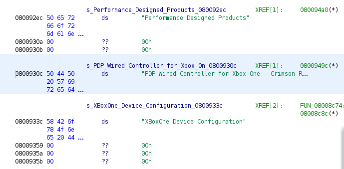
Let’s do a simple patch with the product string, changing it to “Testing Firmware Patches”. The flash can be overwritten with the following commands in the OpenOCD telnet console:
1
2
3
4
5
6
7
8
9
10
11
12
13
14
15
16
17
18
19
20
21
22
23
24
25
26
27
wrongbaud@wubuntu:~/blog/stm32-xbox$ telnet localhost 4444
Trying 127.0.0.1...
Connected to localhost.
Escape character is '^]'.
Open On-Chip Debugger
> flash read 0 bank0-orig.bin
> flash read_bank 1 bank1-orig.bin
flash size = 512 bytes
wrote 512 bytes to file bank1-orig.bin from flash bank 1 at offset 0x00000000 in 0.007867s (63.557 KiB/s)
> stm32f2x unlock 0
Target not halted
stm32f2x failed to unlock device
> halt
target halted due to debug-request, current mode: Handler External Interrupt(67)
xPSR: 0x61000053 pc: 0x0800839c msp: 0x2000ff48
> stm32f2x unlock 0
stm32f2x unlocked.
INFO: a reset or power cycle is required for the new settings to take effect.
> reset halt
target halted due to debug-request, current mode: Thread
xPSR: 0x01000000 pc: 0x080002a4 msp: 0x20010000
> stm32f2x mass_erase 0
stm32x mass erase complete
> flash write_bank 0 bank0-patch.bin
wrote 262144 bytes from file bank0-patch.bin to flash bank 0 at offset 0x00000000 in 3.744948s (68.359 KiB/s)
> reset
>
There are a few steps here that might not make sense, so I wanted to explain them:
- Always, always always take a backup of any flash image before you attempt to reflash.
- See bullet 1
- The STM32 flash controller has a lock bit which keeps prevents unwanted writes. This is set in the “Option bytes” of the STM32
- Luckily for us we were able to unlock the flash, which can sometimes not be an option!
- For the internal flash on the STM32, we need to perform an erase operation before we write to it
- I should add here, that this is never something you want to do if your target is expensive or important unless you’re 100% certain you can return it to it’s original state
- We write the patched firmware image, and restart the CPU, prompting the following to show up in
dmesg
1
2
3
4
5
6
7
[54691.886194] usb 1-6.4: new full-speed USB device number 14 using xhci_hcd
[54691.992411] usb 1-6.4: New USB device found, idVendor=0e6f, idProduct=02a2, bcdDevice= 1.0f
[54691.992417] usb 1-6.4: New USB device strings: Mfr=1, Product=2, SerialNumber=3
[54691.992420] usb 1-6.4: Product: Testing Firmware Patches
[54691.992423] usb 1-6.4: Manufacturer: Performance Designed Products
[54691.992426] usb 1-6.4: SerialNumber: 0000AE38D7650465
[54691.998102] input: Generic X-Box pad as /devices/pci0000:00/0000:00:14.0/usb1/1-6/1-6.4/1-6.4:1.0/input/input28
Excellent - so we now have the firmware fully extracted and loaded into ghidra, as well as the ability to modify it as we see fit…now it’s time to write some macros. But it’s getting late and I almost missed the monthly post deadline for January so I think I’m going to wrap it up here!
Conclusion
When performing an assessment of an embedded system, you typically want to enumerate and explore all possible interfaces and methods of interacting with the target. Whether your end goal is to hunt for bugs, modify the device’s normal operation or just learn more about how it works, hardware debugging is extremely useful. By utilizing hardware debugging we were able to extract the firmware from this target, set up a live debugger and also modify the firmware. Through this this exercise, we also covered how Single Wire Debug works, as well as how to identify, enumerate and debug an unknown CPU with hardware debugging tools. OpenOCD was also used with a FT2232H based interface to extract firmware images as well as reflash new firmware onto the target. Thanks for reading and if you have any questions or just want to talk more about this kind of stuff please feel free to ping me on twitter
Blog Updates (as of 2022):
Future blog posts and entries can be found here.
If you are interested in learning more about reverse engineering check out my 5 day hardware hacking course, public and private offerings are available upon request
Never want to miss an update or blog post? Check out my mailing list for a quarterly newsletter about reverse engineering embedded devices