

Background
To follow up on my last post about SWD and hardware debugging, I wanted to do a deep dive into JTAG from a reverse-engineering perspective. The previous post received a lot of great feedback and it seems that people are interested in this topic, so I wanted to continue the series and expand upon another hardware debugging mechanism. For those who are unfamiliar, JTAG is a hardware level debugging mechanism that many embedded CPUs utilize, with this post I hope to explain how to approach JTAG from a reverse engineers perspective and provide some practical examples along the way.
Goals
With this post, I hope to do the following:
- Explain how JTAG works
- Demonstrate how to discover and utilize a JTAG port/interface on an unknown target
- Provide an overview of some of the current OSS tools that can be used to interact with a JTAG interface
- Utilize JTAG to extract firmware and debug a target
Also, before I give an overview, I wanted to point out a few great resources for learning about JTAG
Blog Updates (as of 2022):
- Future blog posts and entries can be found here.
- If you are interested in learning more about reverse engineering check out my 5 day hardware hacking course, public and private offerings are available upon request
- Never want to miss an update or blog post? Check out my mailing list for a quarterly newsletter about reverse engineering embedded devices
JTAG Overview
JTAG is a hardware interface that was developed to assist developers and testers with low level debugging. JTAG was originally developed for testing integrated circuits and more specifically, sampling IO pins on a target under test. This type of debugging interface allows engineers to test connections on PCBs without needing the probe the physical pin itself. The JTAG interface is controlled via the state machine outlined below:
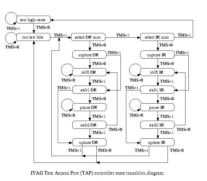
One of the important things to remember about JTAG at this level is that it involves two registers, the instruction register, and the data register. To utilize these registers, the proper states in the above state machine must be entered using the following interface signals:
| Line | Usage |
|---|---|
| TMS | This pin is used to navigate and control the JTAG state machine |
| TDI | Input pin, used to write data to the target |
| TDO | Output pin, Used to read data back out from the target |
| TCK | Used to determine when data is sampled for all inputs and outputs |
| TRST (Optional) | This pin can be used to reset the state machine to the starting state |
The state machine is navigated using the TMS and TCK lines, while data is written to or read from via TDI and TDO respectively. TMS is sampled on the rising edge of TCK, meaning that the TMS line must be asserted before TCK is toggled to navigate through the state machine. Data is then shifted into the instruction register (IR) or data register (DR) depending on the state of the JTAG state machine. When an operation is completed (or after the update DR/IR phase) the resulting data can be shifted out of DR by entering the Shift-DR state. With these primitives in place, manufacturers can implement whatever features they wish over JTAG.
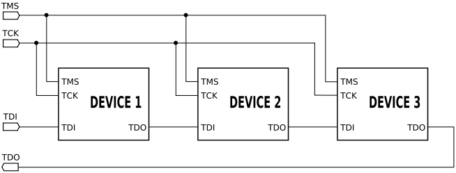
The JTAG standard treats IR and DR as shift registers, and due to this, multiple targets can be daisy-chained together.
In a nutshell, JTAG defines a state machine that is navigated with a minimum of 4 signals. With this state machine in place, end users can write and read from two shift registers, IR and DR.
JTAG Registers
JTAG utilizes two main registers, the instruction register, and the data register. The instruction register is used to determine what function the JTAG controller is about to carry out such as a memory read, or memory write for example. The data register is then used as an additional input to the instruction register, for the previous example, they may be used to provide an address to read from or write to. These registers can vary in size based on their function.
To write to a register one would perform the following steps, we’ll use the IR as an example:
- Enter
Test Logic Resetstate (TLR) (This can be done by asserting theTMSline and cyclingCLK5 times) - Enter
Select IR Scanstate - Enter
Capture IRstate - Enter
Shift IR– This is where we load the data into IR from TDI - Enter
Exit IRstate - Enter
Update IRstate – This stage “latches” the value into IR.
Following this, if there were no data registers required, the operation would be performed, and the result (if any) would be loaded into the data register to be shifted out. However, many instructions require a data register to be filled out as well before operating. In that case, once the data register is written to and updated, the operation will be performed and the result can be shifted out of the data register.
Some instructions do not require the DR to be loaded, for example, if we had loaded the IDCODE instruction into IR (1110b), this would load the processor’s IDCODE value into the data register for us to then clock out and read it on TDO. To read the result out of TDO, one would navigate to the Shift-DR state, and clock in 32 bits on TDI, this would cause the data in the data register to be shifted out on the TDO line. See the image below for a visual representation of what would happen if one loaded the IR with the IDCODE instruction
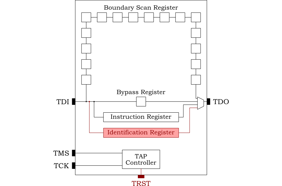
It’s important to remember, that IR and DR can be thought of as shift registers, meaning that when we update them with new values, the old values are then shifted out on TDO.
The JTAG standard defines the following instruction registers:
BYPASS- This instruction connects
TDIandTDO - In the
Shift DRstate, data is transferred fromTDItoTDOwith a delay of oneTCKcycle - 0 is loaded into the data register during the
Capture DRstate - This can be used to determine how many devices are in a scan chain
- This instruction connects
IDCODE- When loaded the Device Code Id Register is selected as the serial path between TDI and TDO
- In the Capture-DR state, the 32-bit device ID code is loaded into this shift section
- In the Shift-DR state, this data is shifted out, least significant bit first
- Core JTAG Concepts
- The state machine is navigated with 4 signals:
TCK,TMS,TDOandTDI TDIis used to provide input,TDOis used for output- Using this state machine data can be shifted into the IR (
Shift IR) and the DR (Shift DR) - The instruction register (
IR) can be thought of as a function, and the data register (DR) can be considered the argument to that function - As data is shifted into
DRandIR, the previous contents are shifted out onTDO - Once data is shifted into these registers, an operation can be performed (entirely dependent on host implementation aside from a few reserved instructions)
- Data is read out of the target by shifting it onto
TDOfrom the data register in theShift DRstate.
- The state machine is navigated with 4 signals:
So now that we have gone over how JTAG works at a low level, we should talk about why we might care about it, and how this interface can grant access to useful features for reverse engineers. One of the most commonly used applications of the JTAG interface is hardware-level debugging (hence the title of this post). This is implemented by the chip manufacturer, and can vary from chip to chip, however, one of the most common implementations of hardware-level debugging for ARM targets is ARM’s CoreSight Debug Interface. This is the same implementation that we communicated with over SWD in my last post, only, in this case, the Debug Access Port is communicated with over JTAG. The specifics of the JTAG implementation can be found here. Luckily for us, some excellent OSS tools can be used to communicate with these ports - this post will focus on using OpenOCD.
OpenOCD takes care of utilizing the JTAG or SWD interface to grant the end-user various primitives that are provided by the debug interface exposed through the CoreSight DAP. The Coresight / DAP architecture is fairly complicated and too much to cover in this (already long) post, so I will potentially save that for another post
JTAG for Reverse Engineers
It’s extremely important to have a solid understanding of the protocol fundamentals when approaching something like this from a reverse engineer’s perspective. When reverse engineering hardware (or software) you want to have your ground truth covered since there are always infinite unknowns. These next few sections will go over how we can take advantage of our low-level knowledge of these protocols to assist us on our path to gaining access to hardware level debugging via JTAG. The first thing that we need to do is determine the pinout, and if the pins exposed allow access to the JTAG interface.
Determining the pinout
JTAG signal lines are often grouped together, sometimes (if you’re extremely lucky!) you will see one of the following headers:

If you find something like this however, it may not have the exact signal groupings, so we will discuss how to determine a pinout if one assumes it’s used for JTAG.
When reverse engineering something like this, you want to start with what you know. Since we know that most manufacturers at least implement IDCODE and BYPASS let’s talk about how we can take advantage of those two instructions.
If you have identified what you believe to be a potential JTAG header or pinout, but do not know the pins, we can use the behavior of these two registers to determine the pinout.
Since the IDCODE register is typically loaded as the default IR, one can test an assumed pinout by doing the following:
- Assign roles to potential output pins (TMS, TCK, etc)
- Enter the
Test Logic Resetstate - Enter the
Select DR Scan,Capture DR,Shift DR - Clock 32 values on
TDIand monitorTDOfor a validIDCODEvalue - Check the
IDCODEvalue that you shifted out if it looks valid congratulations! Otherwise, reassign pins and repeat!
In addition to taking advantage of the fact that the IDCODE register is often loaded into the IR by default, we can also utilize the fact that both the IR and DR behave as shift registers, so if we assume a common register length (32 bits often works) we can attempt to brute force the pinout by doing the following:
- Assign roles to potential output pins (TMS, TCK,etc)
- Using these assumed values, enter the
Test Logic Resetstate - Enter the
Shift IRstate - Shift in a unique 32-bit value on
TDI - Continue to shift 1’s on
TDIwhile monitoring for your unique pattern on TDO (be sure to do this as lease 32 times!). - If the pattern is discovered, congratulations! Otherwise, choose new assignments for the pins and repeat!
Both of these methods are used by the previously mentioned JTAGEnum script, as well as the JTAGULATOR.
Determining Instruction Length
Once you have determined the pinout of the target, then the real fun can begin. The next step is to then determine the length of the IR / DR. To do this, starting with IR, enter the Shift IR state and flood the chain with 1’s on TDI, using a large number like 1024 or 4096, and then clock in a 0. Once this has been done, simply continue to clock in 1’s on TDI, counting the number of clock cycles that it takes before a 0 appears on TDO. This will tell you the length of the IR. Once you have that, you can enter the Shift DR state and repeat the process to determine the state of the DR. This is something that urjtag does very well.
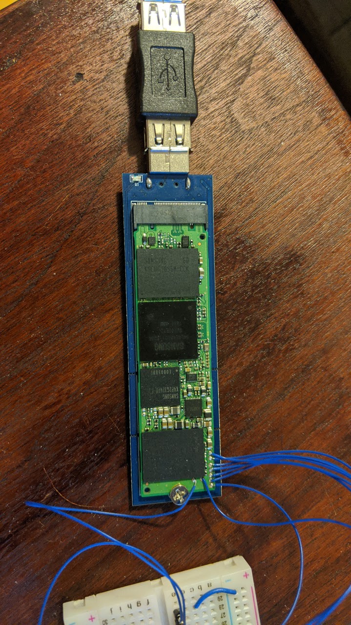
Practical Example: Samsung M.2 SSD
The target for this post is going to be a Samsung M.2 SSD that I recently recovered from an older laptop. After looking at the PCB and spotting what could potentially be JTAG headers, I wanted to outline the process from start to finish.
Practical Example: Locating JTAG Headers / Determining Pinout
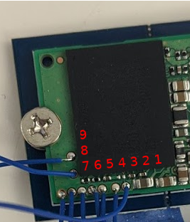
As mentioned before JTAG lines are often grouped - so when looking at a new platform from a hardware perspective, looking for pin groupings greater than 5 is always a good start. Luckily for us on this target, there are 9 vias located along the outside of the PCB. Let’s start by examining the voltage levels of these pins with the drive in a normal operating state
| Pin | Voltage Level | Usage |
|---|---|---|
| 1 | 0.1 V | ??? |
| 2 | 1.8 V | ??? |
| 3 | 0.1 V | ??? |
| 4 | 0.1 V | ??? |
| 5 | 0.1 V | ??? |
| 6 | 0.1 V | ??? |
| 7 | GND | GND |
| 8 | 1.8 V | ??? |
| 9 | 1.8 V | ??? |
From a first pass - these voltage values don’t tell us anything, so what can we determine based on the information we have? First off, we have a GND which is an easy one to determine by using continuity mode on the multimeter and testing against something like a shield of the USB connector (while the target is unplugged of course!). Next, we have one line at 1.8V, typically one would expect this to be TMS as it is recommended to be held high in most documentation.
To determine the pinout, we will use a Raspberry Pi and the JTAGEnum project. This script uses the aforementioned methods to attempt to identify a JTAG pinout. It is also important to note here that the logic levels are at 1.8V so we will need to use a logic level shifter if we’re going to interface to this target. JTAGEnum.sh uses the Raspberry Pi’s GPIO lines to actuate the target interface, in the shell script they include a map of the GPIO values which can be seen below:
1
2
3
# define BCM pins (mapped directly to /sys/class/gpio/gpio${pin[N]})
# 5v 5v  g 14 15 18  g 23 24  g 25  8  7  1  g 12  g 16 20 21
# 3v  2  3  4  g 17 27 22 3v 10  9 11  g  0  5  6 13 19 26  g
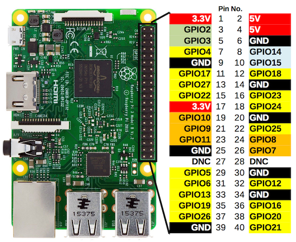
Using our table above, we will wire the following GPIOs to the unknown header:
| SSD Header Pin | RPi GPIO |
|---|---|
| 1 | 2 |
| 2 | 3 |
| 3 | 9 |
| 4 | 10 |
| 5 | 11 |
| 6 | 25 |
In JTAGenum.sh we will modify the pins variable to be as follows:
1
2
pins=(9 11 25 2 3 10)
pinnames=(pin1 pin2 pin3 pin4 pin5 pin6)
Now with the pins wired up, and the logic level shifter in place we can run JTAGenum.sh.
Running the script wired up as shown below yields a TON of results, the output can be seen [here]. Luckily for us, it properly identifies two possible configurations which can be seen below:
1
2
FOUND!  ntrst:pin4 (RPi GPIO 2) tck:pin6 (RPi GPIO 10) tms:pin1 (RPi GPIO 9) tdo:pin3 (RPi GPIO 25) tdi:pin2 (RPi GPIO 11) IR length: 4
FOUND!  ntrst:pin5 (RPi GPIO 3) tck:pin6 (RPi GPIO 10) tms:pin1 (RPi GPIO 9) tdo:pin3 (RPi GPIO 25) tdi:pin2 (RPi GPIO 11) IR length: 4
Next, the script ran an ID scan. You might notice that a lot of results were generated for this, how do we filter through these? There are a few things that you can do to filter through the results, for example, we probably only have 1-2 devices on the scan chain (CPU and flash) so we can immediately ignore those that have more than 2-3 entries. Next, you can rule out those that have long (more than 4-5) sequences of 1’s or 0’s. Luckily in this list, there is an ID that I have seen before: 0x4ba00477 - this ID is for an ARM Cortex core and I’ve seen it before when attempting to get access to Beaglebone Black.
1
2
3
4
5
6
7
8
ntrst:pin4 tck:pin6 tms:pin1 tdo:pin3 tdi:pin2  devices: 1
0x4ba00477
ntrst:pin4 tck:pin6 tms:pin1 tdo:pin3 tdi:pin5  devices: 1
0x4ba00477
ntrst:pin5 tck:pin6 tms:pin1 tdo:pin3 tdi:pin2  devices: 1
0x4ba00477
ntrst:pin5 tck:pin6 tms:pin1 tdo:pin3 tdi:pin4  devices: 1
0x4ba00477
You’ll notice that with the IDCODE scan, the value for TDI varies, that is because this method does not rely on TDI at all so it is a guess.
Luckily some of these results line up nicely with the pattern scan, so we can now assume that we know the pinout of the JTAG interface!
| Pin | Voltage Level | Usage |
|---|---|---|
| 1 | 0.1 | ??? |
| 2 | 1.8 | ??? |
| 3 | 0.1 | TMS |
| 4 | 0.1 | CLK |
| 5 | 0.1 | TDI |
| 6 | 0.1 | TDO |
| 7 | GND | GND |
| 8 | 1.8 | ??? |
| 9 | 1.8 | ??? |
Practical Example: Determining Instruction Length with UrJtag
While OpenOCD is excellent for interfacing with DAP controllers and connecting to debugging cores, the UrJTAG project is great for interfacing with JTAG at a low level. We can use this to detect the various DR lengths with their useful discover command. This method uses the same principles mentioned earlier to select an IR then shift a large number of 1’s into DR followed by a 0, then clocking more 1’s until a 0 is read on TDO!
UrJTAG can use an rc file located at ~/.jtag/rc mine is as follows
1
2
3
4
pi@raspberrypi:~ $ cat .jtag/rc
cable gpio tck=10 tms=9 tdi=11 tdo=25
detect
discover
Below we can see the result of running UrJTAG with these commands:
1
2
3
4
5
6
7
8
9
10
11
12
13
14
15
16
17
18
19
20
21
22
23
24
25
26
27
28
29
30
31
32
33
34
35
pi@raspberrypi:~ $ sudo -E jtag

UrJTAG 2019.12 #
Copyright (C) 2002, 2003 ETC s.r.o.
Copyright (C) 2007, 2008, 2009 Kolja Waschk and the respective authors

UrJTAG is free software, covered by the GNU General Public License, and you are
welcome to change it and/or distribute copies of it under certain conditions.
There is no warranty for UrJTAG.

warning: UrJTAG may damage your hardware!
Type "quit" to exit, "help" for help.

Initializing GPIO JTAG Chain
IR length: 4
Chain length: 1
Device Id: 01001011101000000000010001110111 (0x4BA00477)
  Unknown manufacturer! (01000111011) (/usr/local/share/urjtag/MANUFACTURERS)
Detecting IR length ... 4
Detecting DR length for IR 1111 ... 1 <-- This is BYPASS!
Detecting DR length for IR 0000 ... 1
Detecting DR length for IR 0001 ... 1
Detecting DR length for IR 0010 ... 1
Detecting DR length for IR 0011 ... 1
Detecting DR length for IR 0100 ... 1
Detecting DR length for IR 0101 ... 1
Detecting DR length for IR 0110 ... 1
Detecting DR length for IR 0111 ... 1
Detecting DR length for IR 1000 ... 35
Detecting DR length for IR 1001 ... 1
Detecting DR length for IR 1010 ... 35
Detecting DR length for IR 1011 ... 35
Detecting DR length for IR 1100 ... 1
Detecting DR length for IR 1101 ... 1
Detecting DR length for IR 1110 ... 32 <-- This is IDCODE!
I wanted to highlight UrJTAG in this post because it is extremely useful when looking at a target with a completely unknown scan chain, or DAP architecture. Luckily for us, the IDCODE of this target tells us that it is ARM and we will likely be able to utilize the CoreSight DAP, to do this, we will use OpenOCD. If you are looking at a scan chain where you know nothing about it, I typically start with UrJtag just to get a map of all of the registers. The python bindings for UrJTAG also work quite well and can be used to interface with JTAG at a low level.
JTAG Debugging via OpenOCD.
Since we know the pinout of the JTAG interface on our target, we can now move onto using OpenOCD to communicate with it. I am choosing OpenOCD for this task because it has excellent debugging support for ARM MCUs, particularly the Cortex series which uses CoreSight. The first thing we’ll need to do is choose a hardware adapter, we will use the FT2232H breakout module.
JTAG via FT2232H
With the pinout understood, we can now attempt to talk to the DAP using OpenOCD. For this we will use an FT2232H adapter, for this post I am using a standard FT2232H breakout board. These boards can be used to interract with multiple hardware level interfaces and have excellent software support. You may recall I’ve used them for things such as SWD as well as dumping SPI flash. Using this board, along with a 3.3V to 1.8V logic level converyer we can wire it up to the target as follows:
| FT2232H Pin | Target |
|---|---|
| CN2-7 | TCK |
| CN2-10 | TDI |
| CN2-9 | TDO |
| CN2-12 | TMS |
Next, we will write the outline of our config file, starting with the variables that we know about the target.
1
2
3
4
5
6
7
8
9
10
11
12
13
14
15
16
17
18
19
20
21
22
23
24
25
26
27
source [find target/swj-dp.tcl]

# This is using the name on the SoC
if { [info exists CHIPNAME] } {
  set _CHIPNAME $CHIPNAME
} else {
  set _CHIPNAME s4ln045x01
}

# This is the TAP ID that we discovered in the previous step
if { [info exists CPUTAPID] } {
  set _CPUTAPID $CPUTAPID
} else {
  set _CPUTAPID 0x4ba00477
}

# Set the speed of our adapter
adapter_khz 200
# We are indeed using JTAG
transport select jtag
# We don't have a SRST pin, only TRST it would seem
reset_config trst_only

# Here we create the JTAG TAP/DAP, defining the location and characteristics of our DAP
swj_newdap $_CHIPNAME cpu -irlen 4 -ircapture 0x1 -irmask 0xf -expected-id $_CPUTAPID
dap create $_CHIPNAME.dap -chain-position $_CHIPNAME.cpu
set _TARGETNAME $_CHIPNAME.cpu
When we run openocd with this config file, these are the results:
1
2
3
4
5
6
7
8
9
10
11
12
13
wrongbaud@wubuntu:~/blog/samsung-jtag$ sudo openocd -f minimodule.cfg -f config.cfg
Open On-Chip Debugger 0.10.0+dev-01040-ge7e681ac (2020-01-27-18:55)
Licensed under GNU GPL v2
For bug reports, read
        http://openocd.org/doc/doxygen/bugs.html
Info : auto-selecting first available session transport "jtag". To override use 'transport select <transport>'.
Warn : Transport "jtag" was already selected
Info : clock speed 200 kHz
Info : JTAG tap: s4ln045x01.cpu tap/device found: 0x4ba00477 (mfg: 0x23b (ARM Ltd.), part: 0xba00, ver: 0x4)
Info : Listening on port 6666 for tcl connections
Info : Listening on port 4444 for telnet connections
Info : JTAG tap: s4ln045x01.cpu tap/device found: 0x4ba00477 (mfg: 0x23b (ARM Ltd.), part: 0xba00, ver: 0x4)
Warn : gdb services need one or more targets defined
Now let’s have a look at the DAP, and see if there is any more relevant information in there:
1
2
3
4
5
6
7
8
9
10
11
12
13
14
15
16
17
18
19
20
21
22
23
24
25
26
27
28
29
30
31
32
33
34
35
36
37
38
39
40
41
42
43
44
45
46
47
48
49
50
51
52
53
54
55
56
57
58
59
60
61
62
63
64
65
66
67
68
69
70
71
72
> dap info 0
DAP transaction stalled (WAIT) - slowing down
DAP transaction stalled (WAIT) - slowing down
AP ID register 0x24770002
        Type is MEM-AP APB
MEM-AP BASE 0x80000000
        ROM table in legacy format
                Component base address 0x80000000
                Peripheral ID 0x0000080000
                Designer is 0x080, <invalid>
                Part is 0x0, Unrecognized
                Component class is 0x1, ROM table
                MEMTYPE system memory not present: dedicated debug bus
        ROMTABLE[0x0] = 0x1003
                Component base address 0x80001000
                Peripheral ID 0x04008bbc14
                Designer is 0x4bb, ARM Ltd.
                Part is 0xc14, Cortex-R4 Debug (Debug Unit)
                Component class is 0x9, CoreSight component
                Type is 0x15, Debug Logic, Processor
        ROMTABLE[0x4] = 0x2003
                Component base address 0x80002000
                Peripheral ID 0x04008bbc14
                Designer is 0x4bb, ARM Ltd.
                Part is 0xc14, Cortex-R4 Debug (Debug Unit)
                Component class is 0x9, CoreSight component
                Type is 0x15, Debug Logic, Processor
        ROMTABLE[0x8] = 0x3003
                Component base address 0x80003000
                Peripheral ID 0x04008bbc14
                Designer is 0x4bb, ARM Ltd.
                Part is 0xc14, Cortex-R4 Debug (Debug Unit)
                Component class is 0x9, CoreSight component
                Type is 0x15, Debug Logic, Processor
        ROMTABLE[0xc] = 0x4003
                Component base address 0x80004000
                Invalid CID 0x00000000
        ROMTABLE[0x10] = 0x5003
                Component base address 0x80005000
                Invalid CID 0x00000000
        ROMTABLE[0x14] = 0x6003
                Component base address 0x80006000
                Invalid CID 0x00000000
        ROMTABLE[0x18] = 0x7003
                Component base address 0x80007000
                Invalid CID 0x00000000
        ROMTABLE[0x1c] = 0x8003
                Component base address 0x80008000
                Invalid CID 0x00000000
        ROMTABLE[0x20] = 0x9003
                Component base address 0x80009000
                Invalid CID 0x00000000
        ROMTABLE[0x24] = 0xa003
                Component base address 0x8000a000
                Invalid CID 0x00000000
        ROMTABLE[0x28] = 0xb003
                Component base address 0x8000b000
                Invalid CID 0x00000000
        ROMTABLE[0x2c] = 0xc003
                Component base address 0x8000c000
                Invalid CID 0x00000000
        ROMTABLE[0x30] = 0xd003
                Component base address 0x8000d000
                Invalid CID 0x00000000
        ROMTABLE[0x34] = 0xe003
                Component base address 0x8000e000
                Invalid CID 0x00000000
        ROMTABLE[0x38] = 0xf003
                Component base address 0x8000f000
                Invalid CID 0x00000000
        ROMTABLE[0x3c] = 0x0
                End of ROM table
The first thing that sticks out is that this is a Cortex R4, with this additional information we can create a target in the config file, which should grant access to the MEM-AP allowing for debugging. This can be done by adding the following line:
1
target create $_TARGETNAME.1 cortex_r4 -endian $_ENDIAN -dap $_CHIPNAME.dap
With this additional line, we can try to halt the target via the halt command and read memory via mdw from the OpenOCD prompt:
1
2
3
4
5
6
7
8
9
> halt
MPIDR not in multiprocessor format
target halted in Thumb state due to debug-request, current mode: Supervisor
cpsr: 0x80000133 pc: 0x0001abfc
D-Cache: disabled, I-Cache: disabled
> mdw 0x800000000 10
DAP transaction stalled (WAIT) - slowing down
0x800000000: eafffffe ea000005 ea000006 ea000006 ea00000b e320f000 ea00000e eafffffe
0x800000020: ea0000e3 eafffffe
Here we test stepping through the running firmware:
1
2
3
4
5
6
7
8
9
10
> halt
MPIDR not in multiprocessor format
target halted in ARM state due to debug-request, current mode: Supervisor
cpsr: 0x80000113 pc: 0x0000e10c
D-Cache: disabled, I-Cache: disabled
> step
target halted in ARM state due to breakpoint, current mode: Supervisor
cpsr: 0x80000113 pc: 0x0000e110
D-Cache: disabled, I-Cache: disabled
Success! It appears to be working, and we can single-step through the firmware. Next, let’s use this capability to get some RAM dumps, this page gives an overview of the memory model, so we can use that as a reference. Memory can be dumped to a file with OpenOCD via the dump_image command.
1
2
3
4
5
6
7
8
9
> halt
MPIDR not in multiprocessor format
target halted in ARM state due to debug-request, current mode: Abort
cpsr: 0x200001d7 pc: 0x00000048
D-Cache: disabled, I-Cache: disabled
Data fault registers        DFSR: 00000008, DFAR: 9f7e3000
Instruction fault registers IFSR: 00000000, IFAR: 00000000
> dump_image SDRAM.bin 0x20000000 0xA0000000
> dump_image RAM.bin 0 0xFFFFFFF
Finally, let’s take these RAM dumps and load them into GHIDRA to see if they make sense:
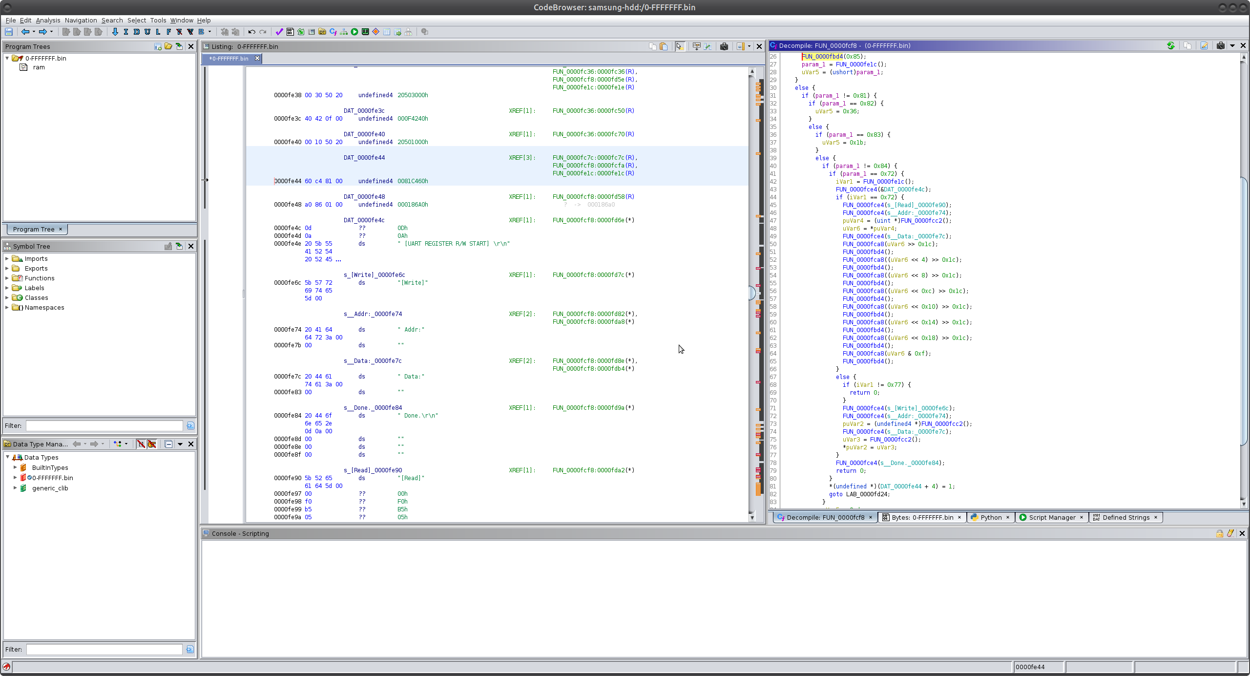
Excellent, we have some xrefs and the init code looks fairly sane. It also looks like there is some sort of debug menu that is presented over the UART, these are likely pins 8/9 on our pinout! Safe to say that this is a valid RAM dump, and with this, I will finish up this post.
Conclusion
This was quite a long post - realistically it probably should have been broken up into 2-3 parts. With this post, we learned how JTAG functions at a low level, as well as how to approach JTAG as a reverse engineer. We were also able to get JTAG access to an undocumented target, extract memory, and single-step through the running firmware. There are lots of things left to do here, like determine if the flash chips themselves can be dumped via JTAG, RE the firmware to look for interesting ways to recover data from the drive (I recently discovered that lots of cool work has been done here already!). As always, if you have any questions or comments, please feel free to reach out on twitter.
Refs
I wanted to mention some awesome work that I found after going through all of this, both of these have already done a lot of what we did in this post today, albeit on slightly different drives. I’m sure that someone on twitter will let me know this so I wanted to link to some excellent previous work that was pointed out to me by some members of the OpenOCD community!
- https://github.com/thesourcerer8/SSDdiag
- http://www2.futureware.at/~philipp/ssd/TheMissingManual.pdf