

Background
In my last post, we managed to dump the firmware off of an Xbox One controller by using the Single Wire Debug interface. Now that we have the firmware image as well as the target CPU determined, we can load it into Ghidra and attempt to learn more about how it works. For this post, we are focusing on learning more about how the firmware image works by writing a proper Ghidra loader and reviewing the USB stack.
Required Reading / Materials
If you’ve not read my last post on SWD and OpenOCD, you want to start there; you also need the datasheet for the target CPU family.
What is Ghidra?
Ghidra is a SRE (software reverse engineering) suite of tools developed by NSA. If you are familiar with IDA-Pro, r2, or Binary Ninja, you are already likely familiar with Ghidra. We can use any of the tools mentioned above to reverse engineer this firmware image. Still, I am choosing Ghidra as it is open source (not unlike r2) and has a relatively robust and well-documented API for scripting and analyzing binaries. Ghidra is also growing with contributions from the community (most notably for me was the addition of the Infineon Tricore architecture to the list of supported CPUs) I have covered utilizing ghidra in previous posts as well and it is quickly becoming my reverse engineering tool of choice.
Loading the Controller Firmware in Ghidra
First off, if you don’t have Ghidra, you can always grab the latest version from here or build it yourself, for this post I am using 9.1.2_PUBLIC release from the official site. We’ll start by opening the CodeBrowser window by clicking on the green dragon button.
After selecting this, you’ll see the following window open up; this is the CodeBrowser
Next, we import the dumped firmware image by pressing I or going to File -> Import File which causes the following window to appear:
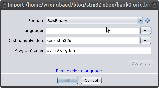
For language, select Cortex (Little Endian), which is what is in the datasheet for this chip. Under options, we set the load address to 0x8000000, which is the appropriate load address for these CPUs according to the datasheet.
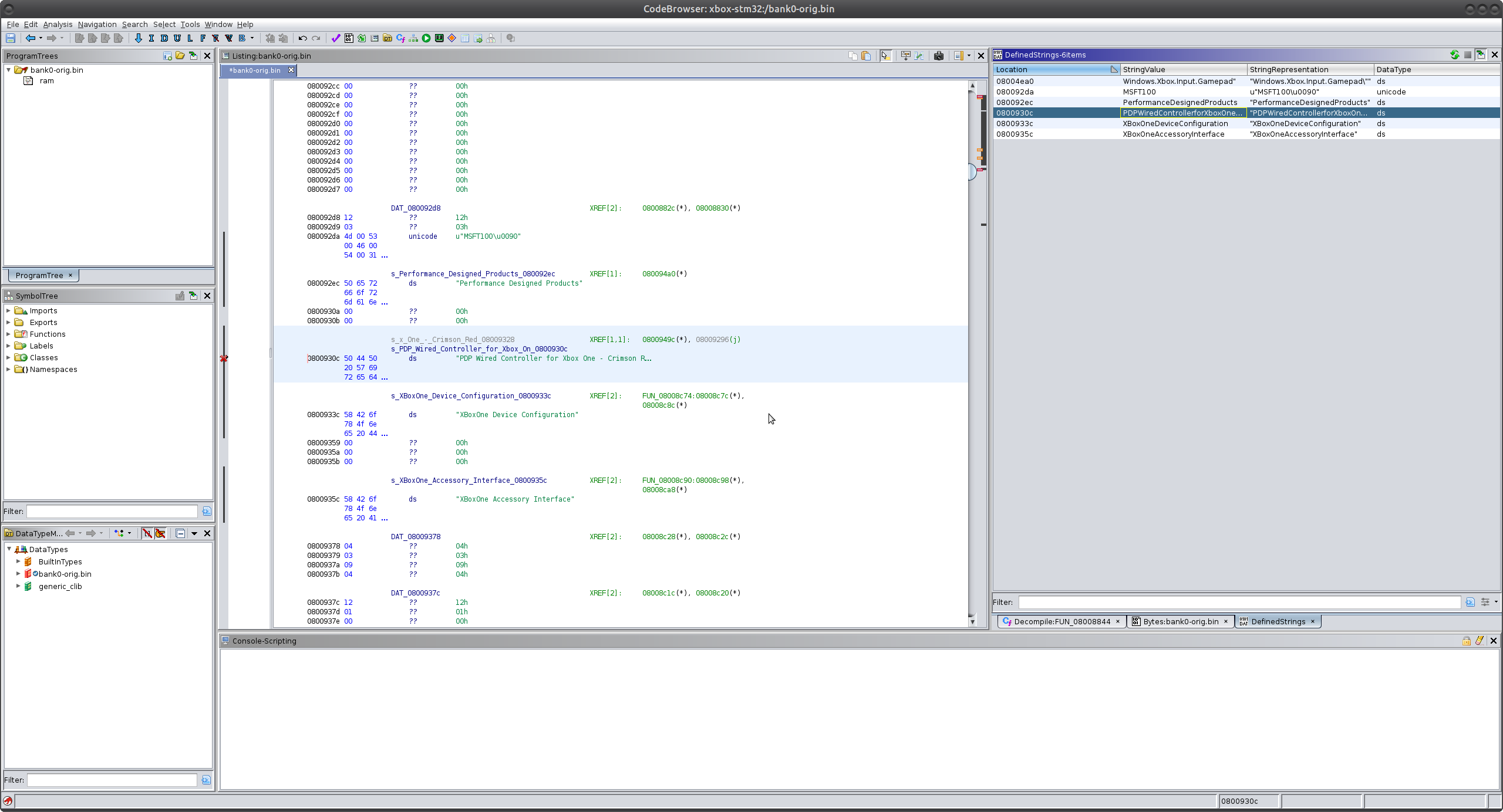
Since this is a rather small firmware image, Ghidra’s auto-analysis handles a lot for us. For example, the USB descriptor strings are assigned XREFs from the start. For those that are unfamiliar, n XREF (cross-reference) is generated when the disassembler detects an address being used by an instruction.
While this is useful, there are still regions of memory that we haven’t yet defined in Ghidra. These are noted by the red values.
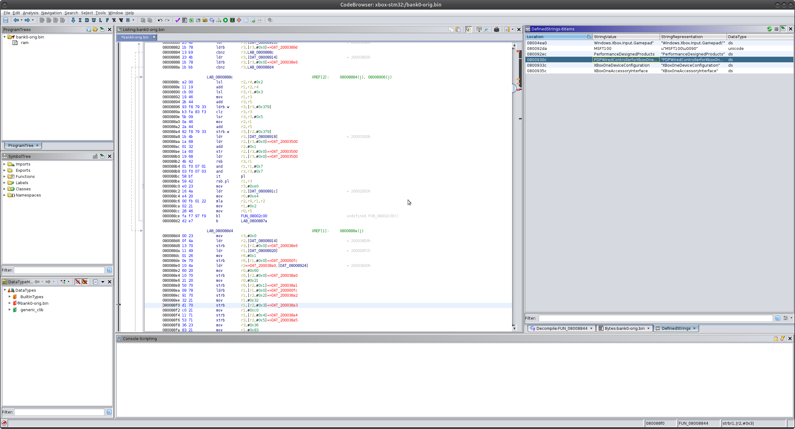
So what are these exactly? These are regions in memory that Ghidra can detect are being used, but are not defined in our Ghidra database. Remember that we are not reverse engineering a standard executable, which would typically reside in virtual memory whose expected ranges are defined in the header (ELF, PE.). This firmware image interacts with various hardware peripherals as memory-mapped IO. In order to make reversing this firmware image a little easier, we can define the memory ranges in Ghidra. This can be done manually, via a script, or through a loader. Since I often run into STM32 variants through my reverse engineering projects, I think it is worth the time to write a simple loader for the STM32F2 series and learn more about extending Ghidra.
What is a Ghidra Loader?
A Ghidra loader is an extension that makes the loading of a binary file more streamlined. For example, if the binary file has a header defining various memory regions and features, the loader can read those features and add the necessary sections to your Ghidra database to assist with the reverse engineering process. For our target, the loader sets up the appropriate memory-mapped peripherals and labeling registers of interest to streamline the process of reverse-engineering the USB stack on this controller.
Writing a Loader
Ghidra has an extension for Eclipse that makes debugging Loaders and scripts reasonably simple, start by downloading and installing the latest version of Eclipse from here. Once you have Eclipse installed and set up, the Ghidra development extension can be installed by following the instructions located at ghidra_9.1.2_PUBLIC/Extensions/Eclipse/GhidraDev/GhidraDev_README.html. With this installed, open Eclipse and go to GhidraDev -> New -> Ghidra Module Project provide a project name and select Loader.
With our loader, we want to perform the following:
- Create and label memory ranges for memory-mapped peripherals
- Find and label entry point and IVT
- Label Locations of Interest
Ghidra Loader Components
When starting with the baseline project, we are given the following function definitions:
getName
This one is fairly self-explanatory, we need not get into it.
findSupportedLoadSpecs
This function is used to determine if your loader can load the binary or not. In this function, you would check the header for your target if it has a known format. For our case with this flat firmware image, there isn’t much we can do here. We do have to set the Language/Compiler pair here, however, which is done with the following line:
1
loadSpecs.add(new LoadSpec(this, 0, new LanguageCompilerSpecPair("ARM:LE:32:Cortex", "default"), true));
Here we are telling Ghidra to use the ARM Cortex LE analyzer.
load
Here we load the actual bytes into the program. In this function we perform the bulk of our loading, we set up our memory map, create any labels, and map the binary data from the ByteProvider object into memory via its InputStream
getDefaultOptions
This function allows you to add custom options to your loader if needed. In our case, we do not need to add any additional options.
validateOptions
Here you can check the custom options to ensure that they make sense, again we aren’t using this for our loader.
Step 1: Create the Memory Map
The first thing we want to do with this loader is to generate an appropriate memory map. To do this, we consult the diagram on page 51 of the datasheet. Given that there are so many, we can create a class for each region, as seen below:
1
2
3
4
5
6
7
8
9
10
11
12
13
14
15
16
        private static class STM32MemRegion {
                String name;
                int addr;
                int size;
                boolean read;
                boolean write;
                boolean execute;
                private STM32MemRegion(String name, int addr, int size, boolean read, boolean write, boolean execute) {
                        this.name = name;
                        this.addr = addr;
                        this.size = size;
                        this.read = read;
                        this.write = write;
                        this.execute = execute;
                }
        }
This way, a region can be defined as shown below:
1
new STM32MemRegion("TIM2",0x40000000,0x3FF,true,true,false)
With this defined, we can create an array memory regions, and then use the following Ghidra API call to create the necessary memory regions in our database:
1
createUninitializedBlock(memregion.name, api.toAddr(memregion.addr), memregion.size, false);
The full loop to create these regions is below:
1
2
3
4
5
6
7
8
9
10
11
12
13
14
15
16
17
18
19
20
21
22
23
24
25
26
27
28
29
30
31
        FlatProgramAPI api = new FlatProgramAPI(program,monitor);
                InputStream inStream = provider.getInputStream(0);
                Memory mem = program.getMemory();
                // TODO: Load the bytes from 'provider' into the 'program'.
                // This is where we actually "Load" the program into ghidra

                // First we loop through our memory map that we created:
                for(STM32MemRegion memregion: STM32MEM) {
                        try {
                                mem.createUninitializedBlock(memregion.name, api.toAddr(memregion.addr), memregion.size, false);
                        } catch (LockException e) {
                                // TODO Auto-generated catch block
                                e.printStackTrace();
                        } catch (DuplicateNameException e) {
                                // TODO Auto-generated catch block
                                e.printStackTrace();
                        } catch (MemoryConflictException e) {
                                // TODO Auto-generated catch block
                                e.printStackTrace();
                        } catch (AddressOverflowException e) {
                                // TODO Auto-generated catch block
                                e.printStackTrace();
                        }
                }
                try {
                        mem.createInitializedBlock("Main Memory", api.toAddr(0x8000000), inStream, 0xFFFFF, monitor, false);
                } catch (LockException | MemoryConflictException | AddressOverflowException | CancelledException
                                | DuplicateNameException e) {
                        // TODO Auto-generated catch block
                        e.printStackTrace();
                }
And with this, we have mapped out all of the memory-mapped peripherals!
Disclaimer: If there is a better way to do this with the Ghidra API, please let me know or even better submit a PR. One of my favorite things about this blog is getting constructive feedback and recommendations from people.
Step 2: Create and Label Entry Point / IVT
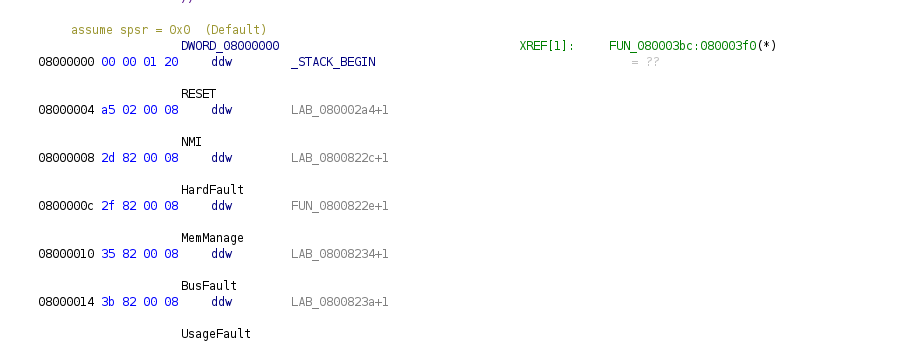
When looking at the datasheet, we can see that the processor maps a memory region to the start address (0x00000000) based on the boot mode. From here, the first entry is the start of the stack address, and the next entry is the reset vector. Following these entries should also be the interrupt vector table.
With our image, it appears to be mapping the flash region 0x8000000 at 0 on boot, meaning that our first DWORD will be the stack size, and the next will be the start address. We can read the data for both of these entries and create relevant labels with the code snippet below:
1
2
3
4
5
6
7
8
9
10
11
12
13
// Top of stack is first value in memory, see page 59 of datasheet
// Make pointer, label it as stack start
int stackAddr = mem.getInt(api.toAddr(0x8000000));
Data stackAddrData = api.createDWord(api.toAddr(0x8000000));
api.createLabel(api.toAddr(stackAddr),"_STACK_BEGIN",true);
api.createMemoryReference(stackAddrData, api.toAddr(stackAddr), ghidra.program.model.symbol.RefType.DATA);

// Mark the entry point of the binary, also referenced in the datasheet on page 59
int entryPoint = mem.getInt(api.toAddr(0x8000004));
Data entryPointData = api.createDWord(api.toAddr(0x8000004));
api.createDWord(api.toAddr(0x8000004));
api.createLabel(api.toAddr(entryPoint),"_ENTRY_POINT",true);
api.createMemoryReference(entryPointData, api.toAddr(entryPoint), ghidra.program.model.symbol.RefType.DATA);
So with this, we can read the initial entries and label them properly with the values from the datasheet on page 59. There are quite a few entries here, so we do the same thing with the IVT that we did with the memory regions, starting with the following class:
1
2
3
4
5
6
7
8
9
10
        private static class STM32InterruptVector{
                String name;
                int addr;
                private STM32InterruptVector(String name, int addr)
                {
                        this.name = name;
                        this.addr = addr;
                }
        }
So with this, we can create another list of IVT entries and loop over them during the loading process. The loop can be seen below:
1
2
3
4
5
6
7
8
9
10
11
12
13
14
15
16
    for(STM32InterruptVector vector: STM32IVT) {
        int ptrVal = mem.getInt(api.toAddr(0x8000000+vector.addr));
        try {
        Data ptrData = api.createDWord(api.toAddr(0x8000000+vector.addr));
        api.createDWord(api.toAddr(0x8000000+vector.addr));
        api.createLabel(api.toAddr(0x8000000+vector.addr),vector.name,true);
        api.createMemoryReference(ptrData, api.toAddr(ptrVal), ghidra.program.model.symbol.RefType.DATA);
        } catch(ghidra.util.exception.InvalidInputException e) {
            // This is ugly, need to fix
            continue;
        }
    }
} catch (Exception e) {
    // TODO Auto-generated catch block
    e.printStackTrace();
}
After adding this, the start of our image now looks like this in Ghidra:
Step 3: Label Locations of Interest
So we want to outline more of the USB functionality in this firmware image, to make things a little more readable, we can label the USB configuration registers. To do this, we do the same thing that we did with the other regions/registers.
To create these, we use a similar technique to the other regions that we identified, except for this time, we only create labels. You can look at the github project for specific details, but the addition of the control registers cleans up the assembly quite nicely.
Closing Thoughts on Loader Development
Writing this Ghidra loader was a beneficial exercise for me because I often end up looking at strange embedded firmware images similar to this one.
If you are wondering why I created classes for each type of region or feature that we added to the ghidra database, I can explain. I end up manually generating memory maps fairly frequently and plan on building a generic loader that loads regions, register labels, and other useful things from a JSON file on startup. I spent far too much time manually entering these regions and creating labels for various esoteric CPUs and wanted to use the STM32 as a learning ground for what it would take to write a loader. After writing this preliminary loader, I think it is feasible to write a generic loader that loads the various memory segments, register labels and other things from a JSON file, but that is for another night!
Analysis
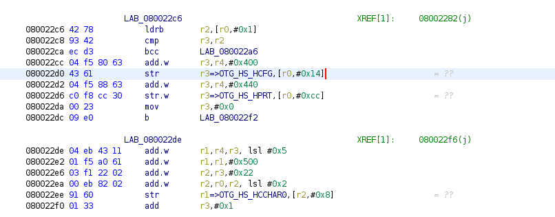
With the new loader, interesting information falls out of subroutines that would otherwise take more time to reverse engineer, take the following example:
Before loader:
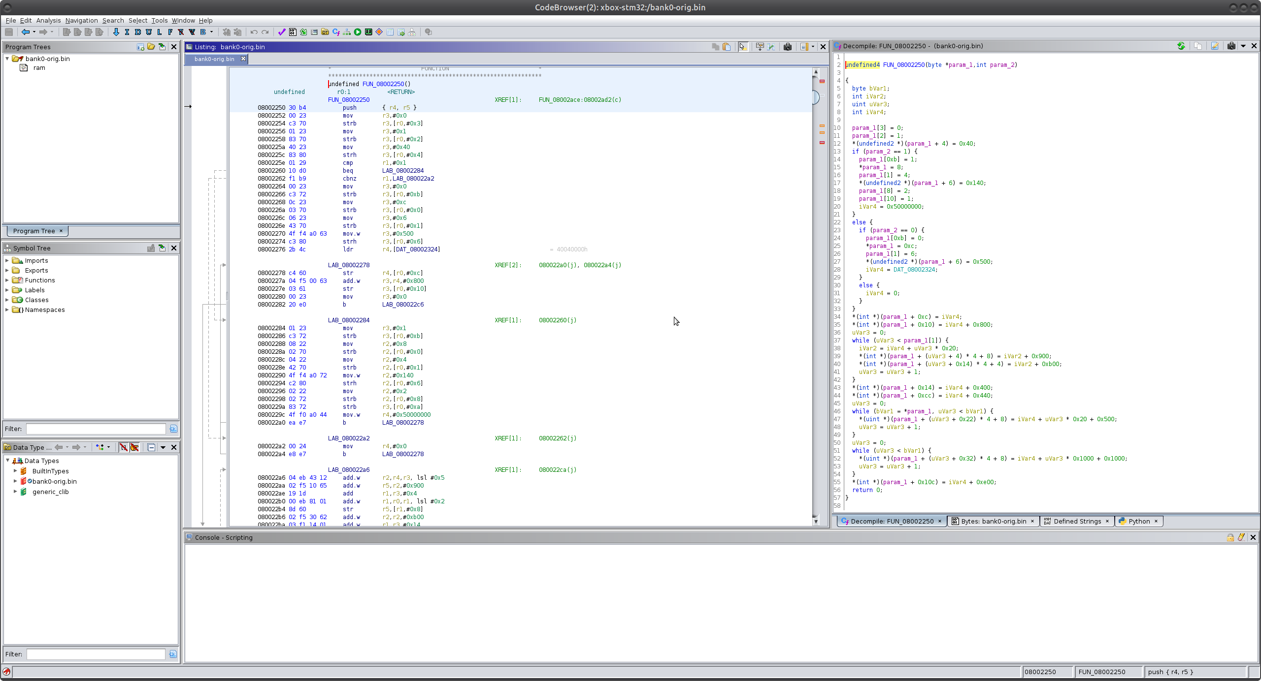
At a glance, it’s hard to determine what this subroutine might be doing. It is accessing memory regions that are not defined, and it’s hard to make heads or tails of the function’s purpose. But after we run it through our loader:
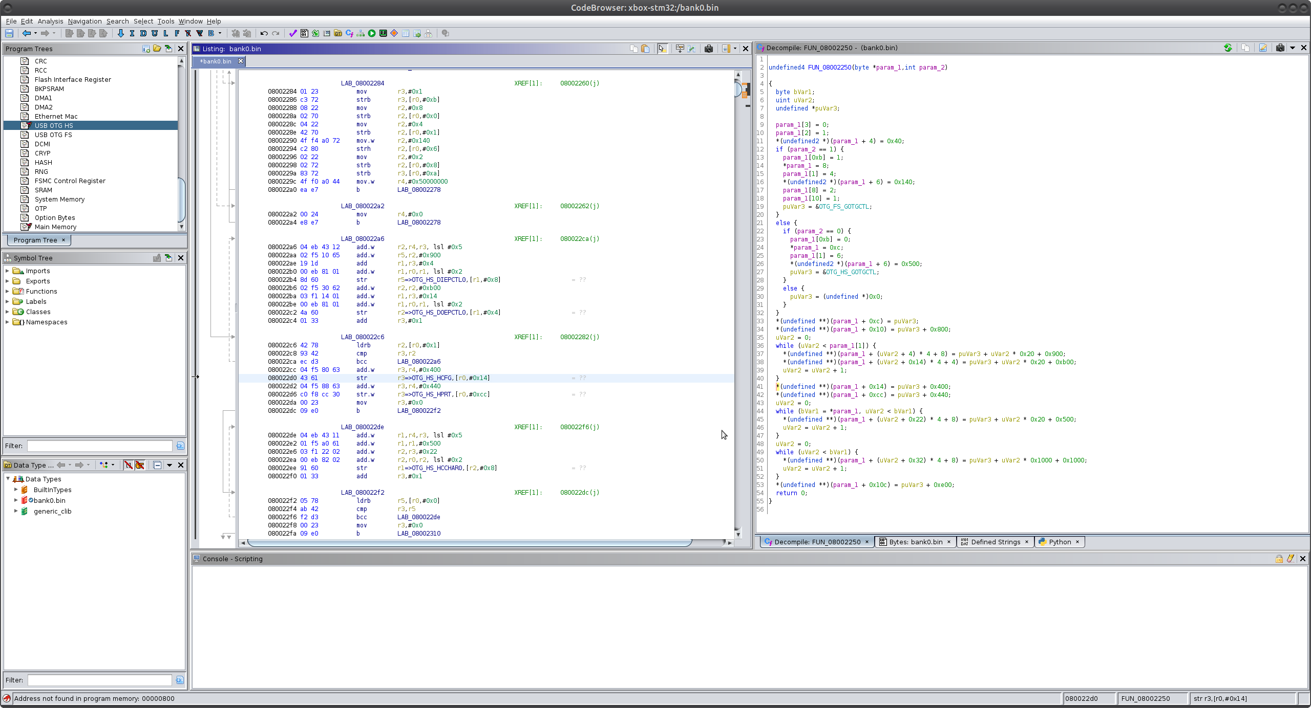
Using the memory regions and the registers of interest, we’re able to see that this function is deciding which USB speed to use as well as setting up the central control registers. Is it perfect? No - of course not, but it does help streamline the process in some way.
There are also far more xrefs generated when using the loader, pointing to things like the various USB descriptors that the device uses during enumeration.
Conclusion
With this post, we put together a simple Ghidra loader for the STM32F2 series microcontroller. While it is certainly not perfect, it was an excellent learning experience, and I hope to get some suggestions/corrections regarding how I implemented things. The loader is on my GH page, and I plan to update it as needed and start working on a more generic loader now that I’ve learned some of the basics. As always if you have any questions or comments, please feel free to reach out to me on twitter
Blog Updates (as of 2022):
Future blog posts and entries can be found here.
If you are interested in learning more about reverse engineering check out my 5 day hardware hacking course, public and private offerings are available upon request
Never want to miss an update or blog post? Check out my mailing list for a quarterly newsletter about reverse engineering embedded devices